Dec 7, 2018 at 6:59 PM Post #241 of 266
Does anybody have a sense of which electrolytics are supplying the ICs? I'd like to replace with 220uf but have no idea how to trace the board. Trace side attached for reference.

26176.jpg
 
Dec 8, 2018 at 2:11 AM Post #242 of 266
You uploaded the wrong pcb side. The power pins are the one in the middle, which should be on the top side.

There seems to be some solders on that IC which look like "cold", Heat up every pin solder on that IC.
 
Dec 8, 2018 at 4:21 PM Post #243 of 266

Not my picture, borrowed it from one of the earlier posts from another user. I don't have the unit with me so can't take a pic of the trace side myself. However, seems that the top layer has the traces I should be following anyway.

I found the schematic for the DAC, but it's in a format I can't access at the moment, sadly (.sch).
 
Dec 17, 2018 at 3:44 PM Post #244 of 266
Quote:

The V-DAC schematic that Barmanekm sent to me is here for anyone to download:

http://www.mediafire.com/?bz5c276k2cb2y0o

TP's supplies might work quite well for this, though I don't know what's their default voltage. For the V-DAC's analog chips you can use +/- 12 to 15v. But you will have to uninstall or desolder the switching booster that powers those chips.
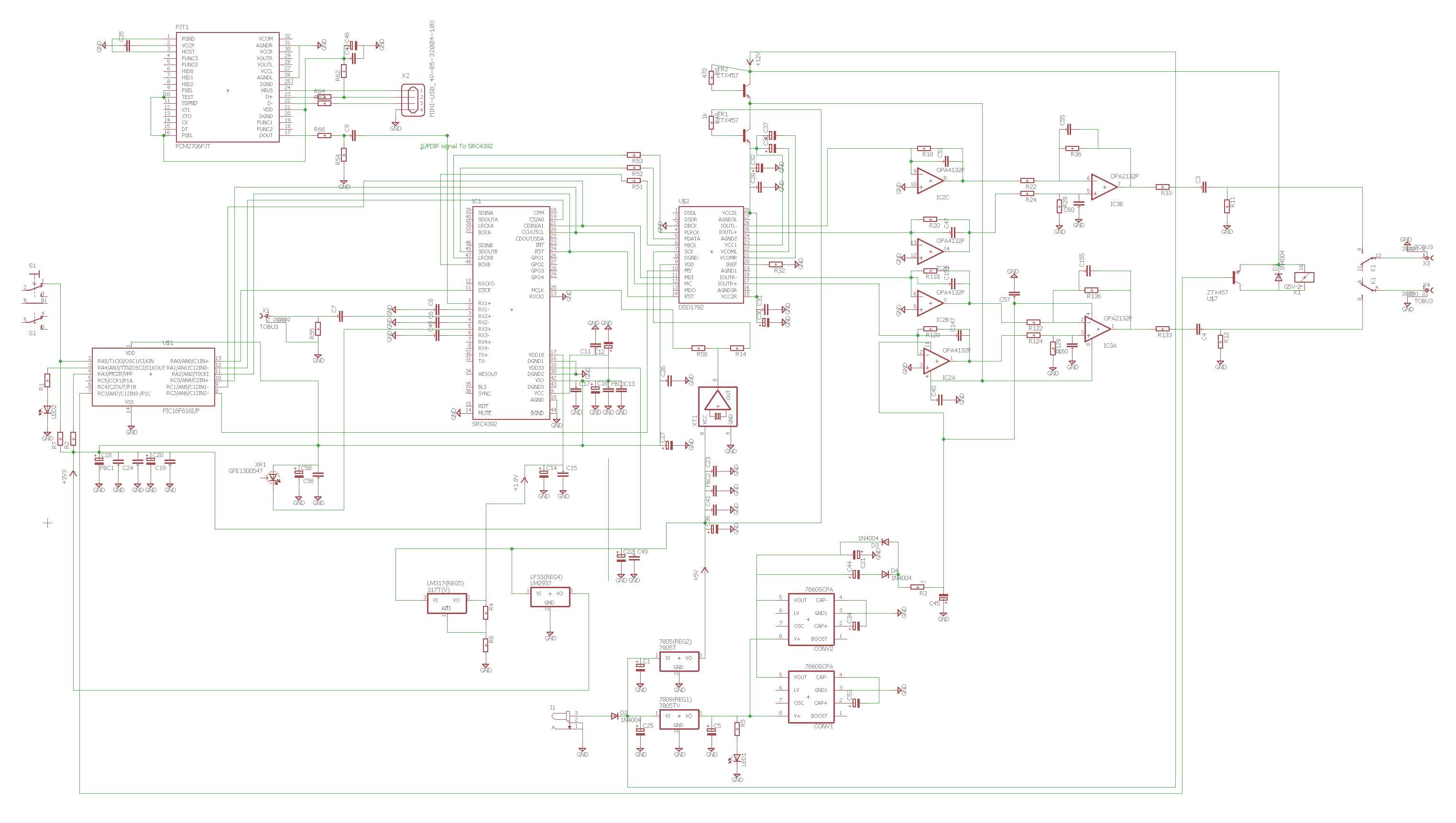
Hi Carlmart -

I downloaded the schematic you posted but can't seem to find a program to open the SCH file. Do you happen to have a screen grab you can share?
 
Dec 18, 2018 at 8:27 AM Post #246 of 266
OK, I got to open the file with Eagle.

This is not the file I had, so I don't remember uploading it to Mediafire.

Unfortunately it has no specs for passive parts, only active. But the ones that matter, like power supply bypass caps at least can be identified.

Have a look at the DAC datasheet and look at the output triple in page 30 and 31. As you can see, they use low offset ICs at the output (LT1028) and no output caps. So if you use one like it or better, you can eliminate your caps too.
 

Attachments

  • V-DAC schematic_small.jpg
    V-DAC schematic_small.jpg
    218.2 KB · Views: 0
Dec 18, 2018 at 8:28 AM Post #247 of 266
V-DAC schematic_small.jpg
OK, I got to open the file with Eagle.

This is not the file I had, so I don't remember uploading it to Mediafire.

Unfortunately it has no specs for passive parts, only active. But the ones that matter, like power supply bypass caps at least can be identified.

Have a look at the DAC datasheet and look at the output triple in page 30 and 31. As you can see, they use low offset ICs at the output (LT1028) and no output caps. So if you use one like it or better, you can eliminate your caps too.
 
Dec 19, 2018 at 5:48 AM Post #249 of 266
Even with the original OPA2132 chip on the V-DAC you would have low offset. Look at the datasheet.

http://www.ti.com/lit/ds/symlink/opa132.pdf

The output caps are sometimes a precaution, even for protection from the following stage eventual DC offset.

But if that stage already has an input cap, it's not necessary. As I already had said, and I took it from Ben Duncan, you should try to design the preamp stages or sources for no caps at inputs or outputs, and put all your money on the power amp input cap. There you should you use the best you can afford, like a propylene os polystyrene type.
 
Dec 19, 2018 at 3:11 PM Post #250 of 266
Even with the original OPA2132 chip on the V-DAC you would have low offset. Look at the datasheet.

http://www.ti.com/lit/ds/symlink/opa132.pdf

The output caps are sometimes a precaution, even for protection from the following stage eventual DC offset.

But if that stage already has an input cap, it's not necessary. As I already had said, and I took it from Ben Duncan, you should try to design the preamp stages or sources for no caps at inputs or outputs, and put all your money on the power amp input cap. There you should you use the best you can afford, like a propylene os polystyrene type.

Perfect. I'm going to remove them later this week, and replace all the ceramic 0.1UF caps with the 2% polyprop Vishays.

However, I'm having a hell of a time reading the schematic. Can you tell which electrolytics are "power coupling caps" for the ICs? I assume they're 100UF pieces, but I can't tell which they are.
 
Dec 20, 2018 at 5:27 AM Post #251 of 266
If you click on the image it will zoom in. The bypass caps are C40 and C57. That is for the quad and dual output ICs,

They seem to be just ceramics, so replacing them with 100uF electrolytics bypassed with 1uF film caps on the copper side might be a good thing.

What's the C30 value on the DSD 1792?

It might be a good thing for you to download the free Eagle version and open the schematic with it. Then you can click on the components and put the values in. Better than drawing them yourself. If possible add the other passive values too.

Then check them with the datasheet. The resistors around the output ICs I wouldn't touch, except if you go for 0.1% precision types. They were certainly hand picked by MF and should be fine. You already changed the filter caps, which is the good thing to do there.

A trick you can try (or even plainly do that only) is not to remove the output caps: just wire bypass them. So if there are any noises you can leave the caps. There shouldn't be, but...

As you can see there's a relay after the cap that controls the RCA outputs, and on CDs there might be a very slight click noise.

Once I had a Sony CD player, which I intend to use again, where I modified the output chip. I don't remember which it was, but it probably wasn't a low offset type. As a result it had very low clicking noises when the CDs began to play.

But the results were so staggering after I bypassed the cap, that I didn't care. It's quite likely I will replace the IC again with a more modern low offset type and see what happens.

If I remember well it didn't have a coaxial interface, to connect it with a DAC, but you could add one. That would be a good comparison to check. The Sony DACs where Burr Brown PCM63s, which were considered one of the best.

This week I received my Topping D50, so I will play with it a bit. The output chips are OPA1612, which some complained sounding a bit "metallic". Burning them in for some time seems to improve on that, but I'm planning some "out of the box" changes, so as not to ruin things inside the very nice box.
 
Last edited:
Dec 20, 2018 at 1:53 PM Post #252 of 266
If you click on the image it will zoom in. The bypass caps are C40 and C57. That is for the quad and dual output ICs,

They seem to be just ceramics, so replacing them with 100uF electrolytics bypassed with 1uF film caps on the copper side might be a good thing.

What's the C30 value on the DSD 1792?

It might be a good thing for you to download the free Eagle version and open the schematic with it. Then you can click on the components and put the values in. Better than drawing them yourself. If possible add the other passive values too.

Then check them with the datasheet. The resistors around the output ICs I wouldn't touch, except if you go for 0.1% precision types. They were certainly hand picked by MF and should be fine. You already changed the filter caps, which is the good thing to do there.

A trick you can try (or even plainly do that only) is not to remove the output caps: just wire bypass them. So if there are any noises you can leave the caps. There shouldn't be, but...

As you can see there's a relay after the cap that controls the RCA outputs, and on CDs there might be a very slight click noise.

Once I had a Sony CD player, which I intend to use again, where I modified the output chip. I don't remember which it was, but it probably wasn't a low offset type. As a result it had very low clicking noises when the CDs began to play.

But the results were so staggering after I bypassed the cap, that I didn't care. It's quite likely I will replace the IC again with a more modern low offset type and see what happens.

If I remember well it didn't have a coaxial interface, to connect it with a DAC, but you could add one. That would be a good comparison to check. The Sony DACs where Burr Brown PCM63s, which were considered one of the best.

This week I received my Topping D50, so I will play with it a bit. The output chips are OPA1612, which some complained sounding a bit "metallic". Burning them in for some time seems to improve on that, but I'm planning some "out of the box" changes, so as not to ruin things inside the very nice box.

Thanks! Burson recommends replacing the "power supply caps" with 220uf pieces. They say that generally, factory pieces tend to be 100uf - since there are quite a few 100uf electrolytics on the board, I'm having a hard time reading the schematic to tell which are "power supply caps."

I think the bypass caps, C40 and C57, are fine as 0.1uf film caps.

C30 is a 10uf.

I'm just going to remove the caps entirely this weekend and replace with some 18 gauge wire - if it's no good, I can always replace them.

Let us know how the Topping comes out!
 
Dec 20, 2018 at 5:16 PM Post #253 of 266
If you already have those 220uF for the Burston, that power pins bypass is shared between the quad and the dual (Burston) chips. If you can replace the 0.1uF bypasses with 1uF types, as they might improve things better .

But I think you should try replacing the output bypasses with a 220uF + 1uF combo for the bypasses. You solder the 220uF on the top side, and the 1uF cap on the copper side. The 220uF cap should be good quality, and may improve the bass.

There are two sets of capacitors for the DAC: C28-C32 and C30-C31. Each set is close to pins 15 and 28. This is very important: the bypass caps being close to the pins.

That should also be the case with the output ICs bypasses. They sharing bypass caps and with such small values seems like unnecessary savings. The ideal thing might be to try two caps for each and also increase the larger value up to 470uF, but listening to the DAC when you increase the values from 100uF up to 470uF. Then you can listen to any change.

For the DAC bypassing, going up to 100uF could be good thing, but this time using Os-Con caps. The ones you find now are SMD types, but you need through hole types. Perhaps these might do:

https://www.ebay.com/itm/10-pcs-SAN...906630?hash=item3f7d868186:g:72cAAOSwblZZKPQH

Os-Cons are usually recommended for digital stages, not for analog ones.

About the output caps: do not extract them if you can. Just solder a wire between the pins. The ideal thing might be for you to clip alligator clips between the pins to bypass them, and listen to the results with and without them.

You could even bypass the output relay entirely for this test, using alligator clips (or even two coaxial cables) to go from R11 and R12 directly to the output RCAs. That would eliminate the relay contact.
 
Dec 20, 2018 at 5:53 PM Post #254 of 266
If you already have those 220uF for the Burston, that power pins bypass is shared between the quad and the dual (Burston) chips. If you can replace the 0.1uF bypasses with 1uF types, as they might improve things better .

But I think you should try replacing the output bypasses with a 220uF + 1uF combo for the bypasses. You solder the 220uF on the top side, and the 1uF cap on the copper side. The 220uF cap should be good quality, and may improve the bass.

There are two sets of capacitors for the DAC: C28-C32 and C30-C31. Each set is close to pins 15 and 28. This is very important: the bypass caps being close to the pins.

That should also be the case with the output ICs bypasses. They sharing bypass caps and with such small values seems like unnecessary savings. The ideal thing might be to try two caps for each and also increase the larger value up to 470uF, but listening to the DAC when you increase the values from 100uF up to 470uF. Then you can listen to any change.

For the DAC bypassing, going up to 100uF could be good thing, but this time using Os-Con caps. The ones you find now are SMD types, but you need through hole types. Perhaps these might do:

https://www.ebay.com/itm/10-pcs-SAN...906630?hash=item3f7d868186:g:72cAAOSwblZZKPQH

Os-Cons are usually recommended for digital stages, not for analog ones.

About the output caps: do not extract them if you can. Just solder a wire between the pins. The ideal thing might be for you to clip alligator clips between the pins to bypass them, and listen to the results with and without them.

You could even bypass the output relay entirely for this test, using alligator clips (or even two coaxial cables) to go from R11 and R12 directly to the output RCAs. That would eliminate the relay contact.

If I replace the 0.1UF bypass caps with 220UF, the ones I have are polar. Does it matter which direction the polarity goes?

And as to the output caps, all I need to do I link the pins with a length of wire on the copper side?
 
Dec 20, 2018 at 6:24 PM Post #255 of 266
Oh, you mean regular electrolytics? They have to be oriented in polarity, or they would explode.

You can see the marked polarity on the cap body. You can use a meter on the ceramic cap to see where is the + and where is the -, and solder the electrolytic accordingly. The ceramic s wire terminals are exposed, so that shold be easy.

Use a marker, red and black if you want to or just (+) (-) symbols written on the pcb. With a meter you find each cap polarity and mark it on the pcb. Remove the ceramics and replace them with the electrolytics.

If you want a larger schematic of the parts you will be working on, I can provide it.

About the output caps, yes, just use a length of wire on the pcb side. You can also try what I told you, completely bypassing output capacitor and output relay. Removing the wires later should be easy. Be careful with shorts or cold solders.
 

Users who are viewing this thread

Back
Top