


tangent
Top Mall-Fi poster. The T in META42.
Formerly with Tangentsoft Parts Store
- Joined
- Sep 27, 2001
- Posts
- 5,969
- Likes
- 58
Quote:
Yes. They're spaced for the now-discontinued Modified Linkwitz Crossfeed board.
Quote:
Yes, as long as you're careful.
The easiest guide for a safe cut is to just cut off the "tabs" containing the mounting holes.
You can actually cut a little deeper than that, right along the line of the rear-most diode inline with the trace from WALL +, but you risk nicking traces.
Either of these cuts will expose copper, so be careful not to touch anything metal to that raw board edge. You might want to re-insulate it.
Oh, and don't breathe the dust.")
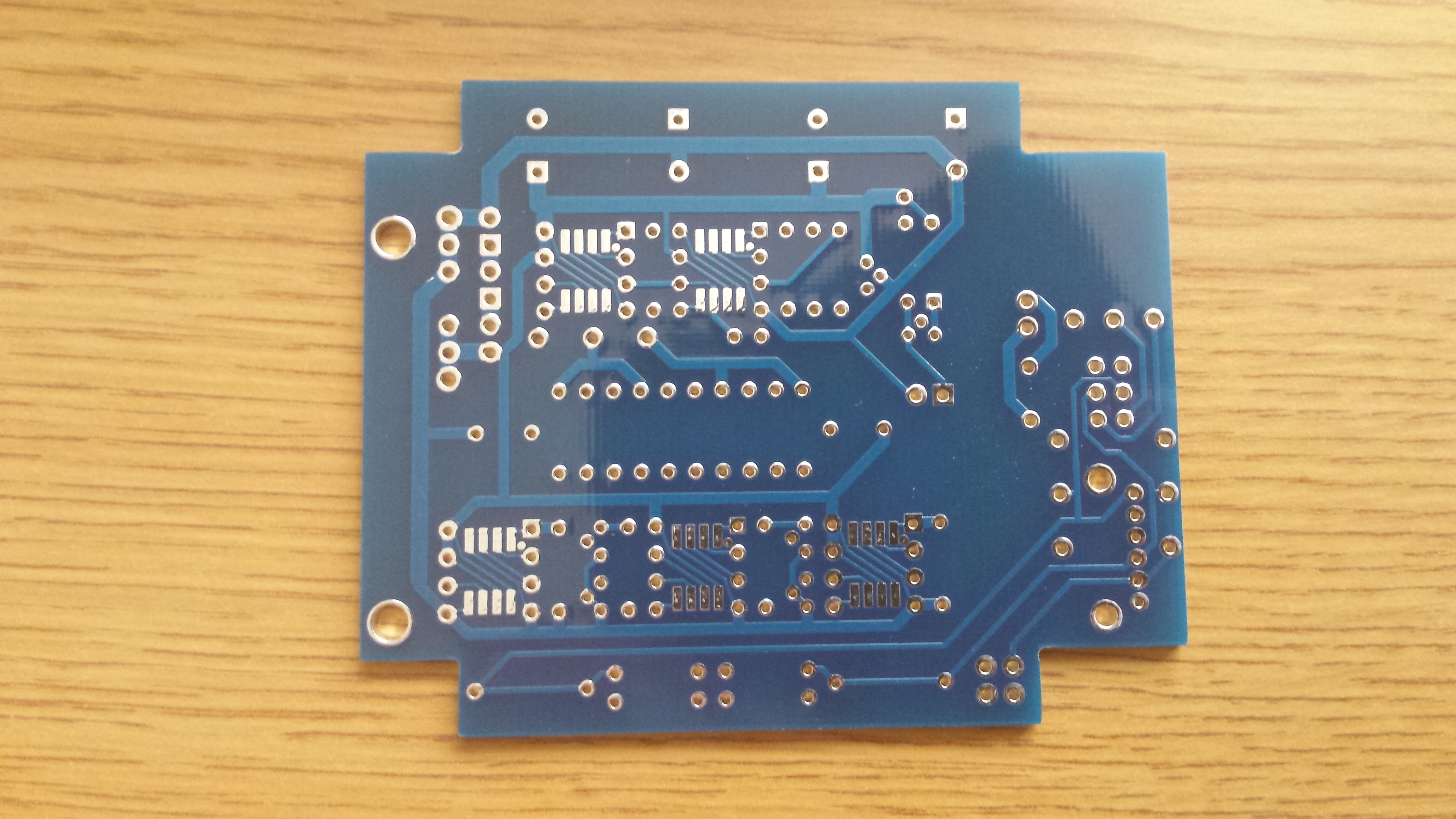
At the bottom of the board there are four holes. Are these for mounting a daughter board?
Yes. They're spaced for the now-discontinued Modified Linkwitz Crossfeed board.
Quote:
Can these be cut off?
Yes, as long as you're careful.
The easiest guide for a safe cut is to just cut off the "tabs" containing the mounting holes.
You can actually cut a little deeper than that, right along the line of the rear-most diode inline with the trace from WALL +, but you risk nicking traces.
Either of these cuts will expose copper, so be careful not to touch anything metal to that raw board edge. You might want to re-insulate it.
Oh, and don't breathe the dust.

