the Pimeta-V2 thread
Apr 13, 2009 at 1:38 PM Thread Starter Post #1 of 651

linuxworks

Member of the Trade: Sercona Audio
Joined
Oct 10, 2008
Posts
3,456
Likes
68
since 'the other forum' seems still to be down, lets talk about the pimeta-v2 here.

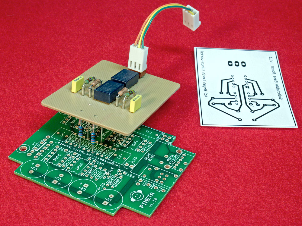
I just built my prototype last nite. some pics:

3436163126_87e090f3fe_o.jpg


3436163960_63046e1c77_o.jpg


3435358531_11f7ce5c33_o.jpg


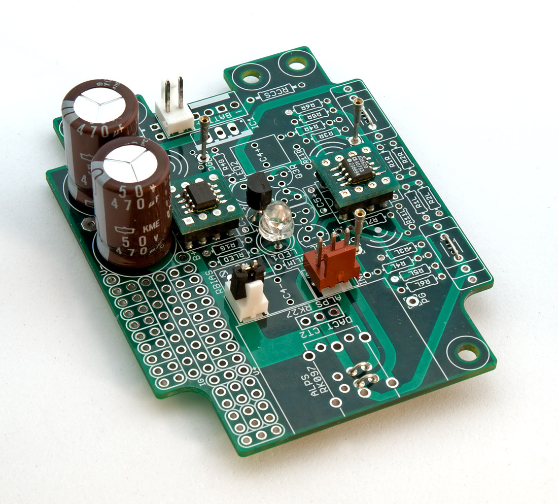
I opted to go with a 'mostly SMD' build ... all the fun stuff is underneath
wink.gif


one thing that I wasn't 100% sure of and needed to check the spec sheets on; I used tantalum smd caps and they mark the band with the PLUS side of the cap not the minus! I did recall that they were the opposite of eletrolytics but its probably worth mentioning in the instructions just for safety sake.

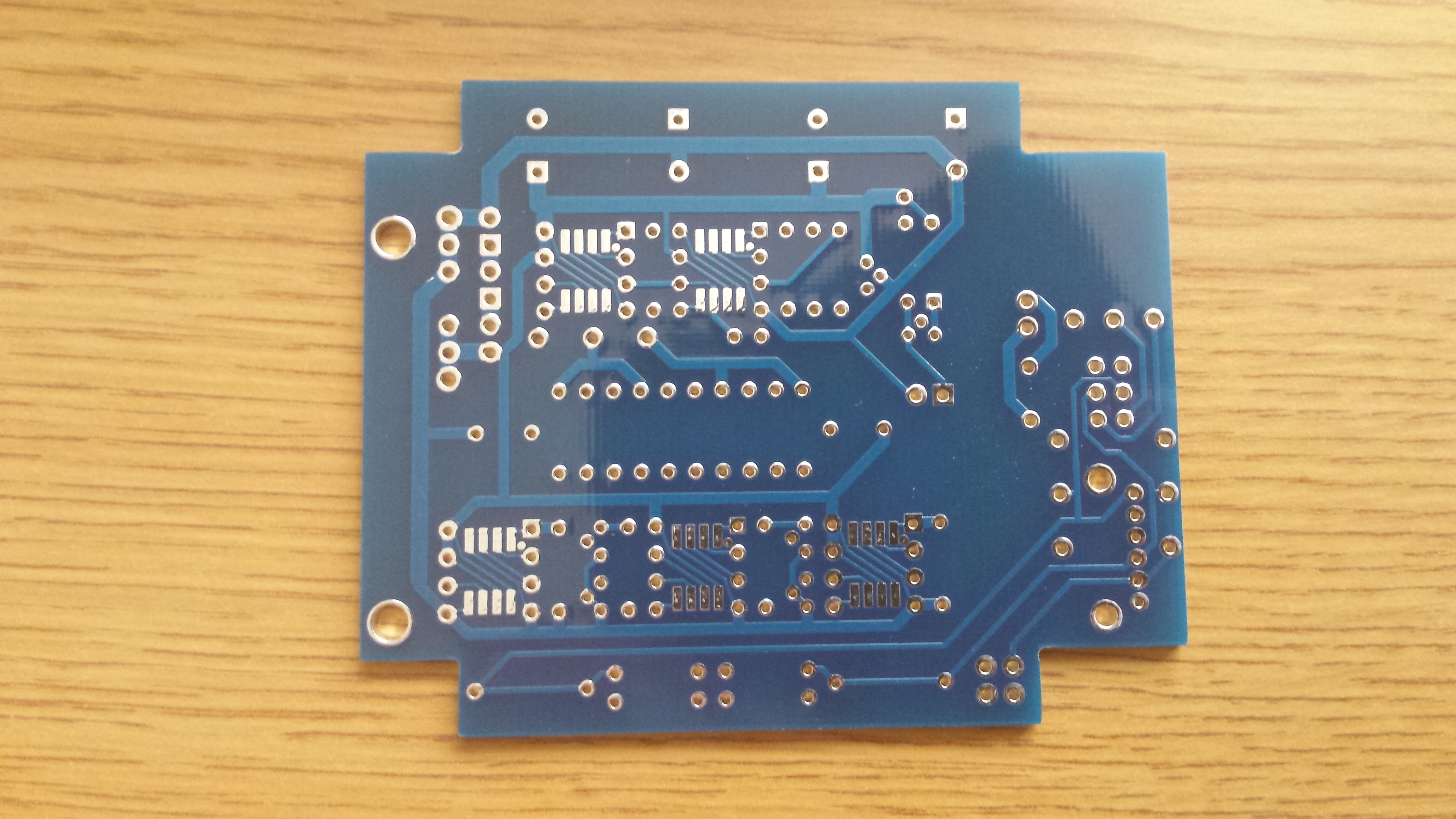
I wasn't sure if I had a solder bridge on the pads that hold the tant caps but it appears the resist did its job. still, I would have liked a bit more void around the copper pads on parts like that. once a tant or diode is soldered down, its hard to tell if there is excess solder that could short or not.

also, I'd suggest adding or moving the index dots (plus signs or dots for chips or other indexing silkscreen) so that even when the parts is installed, the legend isn't covered. this helps desk-checking or magnifier checking without having to have a board layout printout handy. example would be the smd buffers - once they are installed, the silkscreening is completely covered and you can't see where the index dot is anymore. minor detail, though - but if there is going to be another rev before its final, I'd like to suggest this slight silkscreen change.

I have not used the proto area yet. still thinking what my first hack will be for that section of the board
wink.gif


I used the default gain as spec'd in the schematic. on my sony mdr-v6 phones (my junk ones that are 'ok' to blow up on testing) I noticed more hiss than I'd want, on pause. however on my senn hd650 it sounds fine so it was probably a gain issue. on my next build I might lower the gain a bit or just provide switchable gain via relay-paralleling R's at the R4 spot.

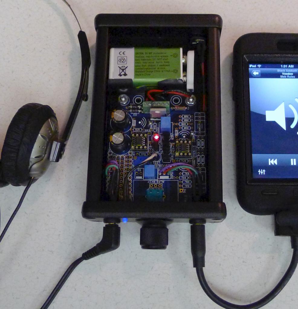
the pimeta is being fed 24v from a TREAD that also supplies voltage to my volume control chip (burr brown PGA chip thing that I'm also working on). when I tested it at 9v, it sounded 'just fine' also, so I guess it passes the portables voltage test, too.
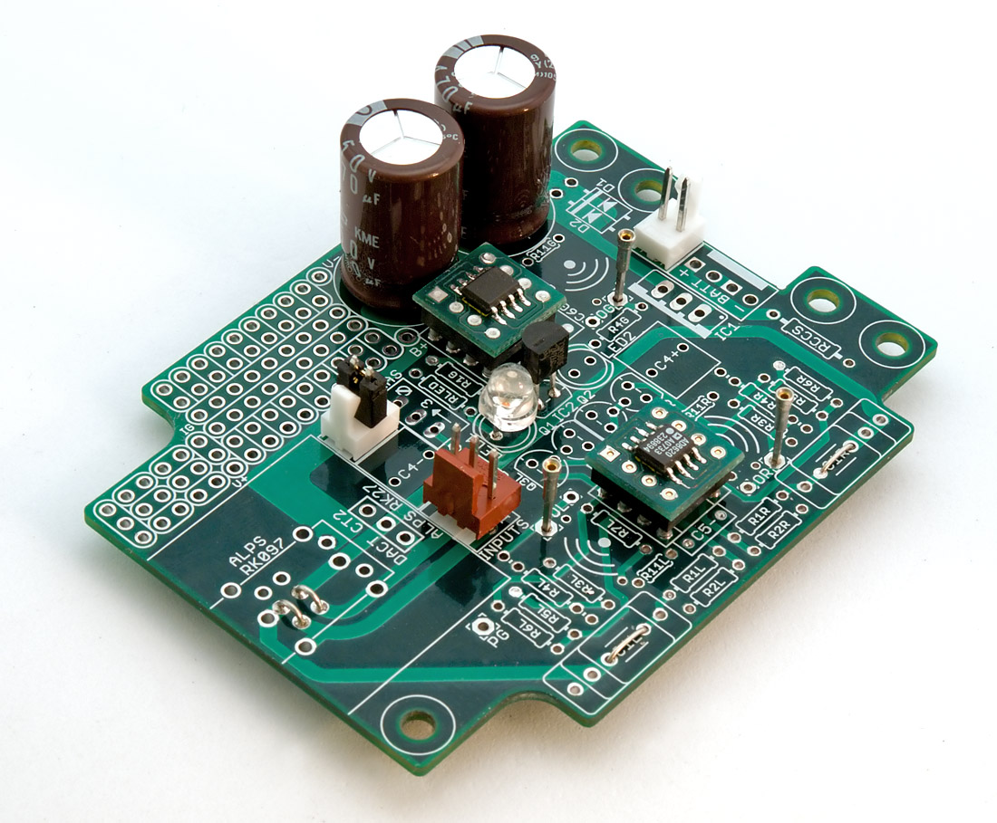
 
Apr 13, 2009 at 4:50 PM Post #3 of 651
Looks nifty... but haven't you always insisted 470uf per rail is "too little", in a Pimeta?

Quote:

once a tant or diode is soldered down, its hard to tell if there is excess solder that could short or not.


That's what multimeters are for.
 
Apr 13, 2009 at 5:31 PM Post #5 of 651
its a 4 layer board, for one. so I think more 'planing' is there and that's supposed to be a Good Thing(tm)
wink.gif


no more need to cut traces on the input cap pads. now you either elect to install a cap OR you install a jumper (I went with the jumper, for now). but no more taking a knife to the pretty pcb to pick cap or capless
wink.gif


there are more spots that are designed-in for molex headers. I made use of quite of few of them. one of them is a power switch and I elected to install headers AND put in a jumper shunt, just to remind me and also provide a real easy manual 'stop button' if I was under the cover and troubleshooting a system that had this pimeta 'module' installed. or if you really do want a power switch, this is the place to connect it.

there is a whole proto area (scratch pad) that has power rails and room for a large DIP there (or perhaps 2 smaller dip8's). or more rail cap. or other things. I left mine alone. for now
wink.gif


the buffers now mount SMD style and they benefit from having solder pads or 'pillows' under them. these buffer chips have metal heat pads built into the chips and so having those 2 touch makes good heat dissipation sense. there is no DIP way to do the buffers anymore so SMD is a must, now. the 2 opamps are still DIPable if you want and they also have SMD pads undeneath if you wanted to go all SMD for the chips.

the transistors for biasing are not SMD (sniff) and I didn't install mine yet. I plan to but not on the first pass. there is a pot, now, that adjusts the bias for both and one of the 2 LEDs is 'part' of the biasing, now.

there is formal support for battery and trickle charging with a lm317 onboard.

(that's just off the top of my head)
 
Apr 13, 2009 at 5:34 PM Post #6 of 651
Quote:

Originally Posted by Nemo de Monet /img/forum/go_quote.gif
Looks nifty... but haven't you always insisted 470uf per rail is "too little", in a Pimeta?


me? I never insist. do I?
wink.gif


I picked what I had that had a high voltage on it. I planned to use a dual 12 or dual 15 and didn't want to skimp on getting too low a safety margin on the cap. plus, these fit the holes well
wink.gif


Quote:

That's what multimeters are for.


I disagree. ideally, it is preferable to know from just looking (even with naked eye and no magnifier) if its 'good' or not. that's one of my litmus' for a perfect design.
 
Apr 14, 2009 at 1:10 AM Post #7 of 651
Excellent photos as usual, linux.

I'm going for an SMD PIMETA v2 as well, but I'll probably populate more of it than you did such as the volume pot and class A. I really like the through-hole/SMD duality because it makes troubleshooting easy when going the SMD route. I actually asked tangent if it were possible to configure the board to allow a DC regulator. Of course, there would have to be some tweaking on the user end. I was thinking of using the LM317 as a regulator instead of as a CCS for the battery, and it could easily be done with the prototype board. Simply omit the diodes, solder pins ADJ and Vout to the board while leaving the Vin in the air, bridge Vout with the Vin/B+ trace, and air-wire resistors, diodes and capacitors accordingly as per the datasheet. An even easier regulator would be to use the LM78xx series of regulators, and that would do away with the air-wiring and parts count. There is a small line up of Xicon linear unregulated wall AC/DC supplies available at Mouser, so that will be part of my PIMETA v2 prototype plans. Any ballpark figures for current draw, linux? I may go with 3x OPA627 off the bat, and that should send my max current draw somewhere around the 100mA area. Mind you, those are from the max readings when operating at +/-15V. Would it make sense to use an LM7824 with an unregulated 24V wall wart? I know the unloaded voltage will be a bit higher than 24VDC, but I wonder if the LM78 would stay in regulation as it has a 2.0V dropout. I could easily go with the LM7818, but I just want to know if I could pull off 24V. I likely wouldn't be able to hear the difference anyway. I only need a gain around 2-3, so I likely won't need all that much extra voltage swing on my low-ohm headphones.

Edit: Also, wouldn't you rather just jumper from the inputs to R1? It may not be as clean, but you shorten the signal path and blah blah blah. Just a thought.
 
Apr 14, 2009 at 3:47 AM Post #9 of 651
You need a kit? The old PIMETA didn't even have one.

Looking at the board and LM78xx datasheet a little harder, you can insert all three TO-220 terminals right in there with a few sleights of hand. Omit the diodes from the board again, throw in the LM78xx, and omit RCCS and the Molex connectors for the battery and the wall input. Then wire in the wall power into the WALL input holes; just bridge the diodes' anodes (non-striped ends) and jumper the wall V- to the hole for RCCS that's nearest the R in RCCS. Then you get to use the remaining battery Molex holes for the input capacitor for the LM78xx with more creative wiring.

Schematic
Board layout
LM317 datasheet
LM78xx datasheet

Surely, this is a deviation from the original powering options for PIMETA v2, and I can see this kind of thing mucking up a beginner's understanding of the amp with the different power supply choices. Approach this option with caution unless you're sure of what you're doing. We still don't know what the final board will look like, so don't throw all your eggs in this basket just yet. I'm merely exploring the possibilities as the board stands.
 
Apr 14, 2009 at 1:28 PM Post #12 of 651
If you check the schematic and board layout, there's room for a bass boost incorporated into the amp already. That's why there's an extra set of holes for R4LR. Hm, maybe I'll try bass boost with my amp too.
 
Apr 14, 2009 at 1:35 PM Post #13 of 651
if you notice, I lifted the red input connector off the pc board a bit. if you install it flush, it covers the silkscreen lettering/legend and I wanted to be able to see that ground wasn't in the middle (as I normally make plugs like this) but on one side. if I covered up the lettering I would probably make a cable incorrectly for this module; if not now, then later. I know myself too well
wink.gif
so I allow the lettering to be seen by this 'cue'.

same issue with the battery molex - except that there are some more holes to one side and that shows the left/right plus/minus labelling which applies to the smaller 'wall' connector as well. still, I do prefer all *important* labelling to be visible even when a component is installed. I guess this is an eagle library issue (?)
 
Apr 14, 2009 at 1:41 PM Post #14 of 651
I'm planning on having some relay switchable bass-boost in a few levels. not sure how to mount the relays yet (in air or on the scratchpad) but switchable levels of BB is one of the things I like about this design. I made an early hack here:

http://www.head-fi.org/forums/f6/bas...ke-ppa-393311/

3195734440_c83189c85e_o.jpg


and I might try something similar again on the v2. maybe even more relays, for more finer grained levels (selectable) of boost. a binary code to 'address' the r/2r resistors would give 2^n levels of selection
wink.gif
 
Apr 14, 2009 at 2:28 PM Post #15 of 651
Quote:

Originally Posted by Earwax /img/forum/go_quote.gif
This looks great. I hope it will be possible to use the scratch pad area for a bass boost?


From Tangent's docs:

Quote:

One of the most popular features of the PPA is its bass boost circuit. The cool thing about it is that it uses the op-amp circuit that already had to be there and it’s completely bypassable. As audio filters go, it’s about as problem-free as you could hope for.

There are a couple of ways to get bass boost with the PIMETA v2.

The first way is hinted at on the schematic. There are two extra pads off the ends of the thru-hole footprint for R4, plus the SMT pads on the bottom side. This allows for up to 3 components here, a resistor, a cap, and a switch. This is enough to give us a weaker form of bass boost than in the PPA, which I call “unity boost.” The difference is, the resulting amp is effectively just a unity-gain headphone driver with bass boost. This is fine for many situations. Most sources these days have enough voltage to drive headphones; they’re just current starved and have too high an output impedance to drive high-quality headphones to their full potential. A PIMETA in unity gain solves that problem. If you do this, I recommend using the outer pair of holes for the caps, the inner pair for the switch, and the 1206 SMT pads on the bottom side for the R4 resistor.

If you really do need voltage gain, you can still get a PPA-style bass boost. The thing you need, which we didn’t have room for on the PIMETA v2 board, is what the PPA calls R7: a resistor in series between the buffer output and R4. You can do this by running two pairs of hookup wires from the ends of R4R and R4L to the scratchpad area, then build out the bass boost circuit there. The needed changes will be obvious with a little study of the PPA schematic. Alternately, you can build this R7+R4+cap+switch circuit on a small chunk of perfboard and mount it vertically, like an add-on card in a PC, in the R4 thru-hole pads.


Users who are viewing this thread

Back
Top