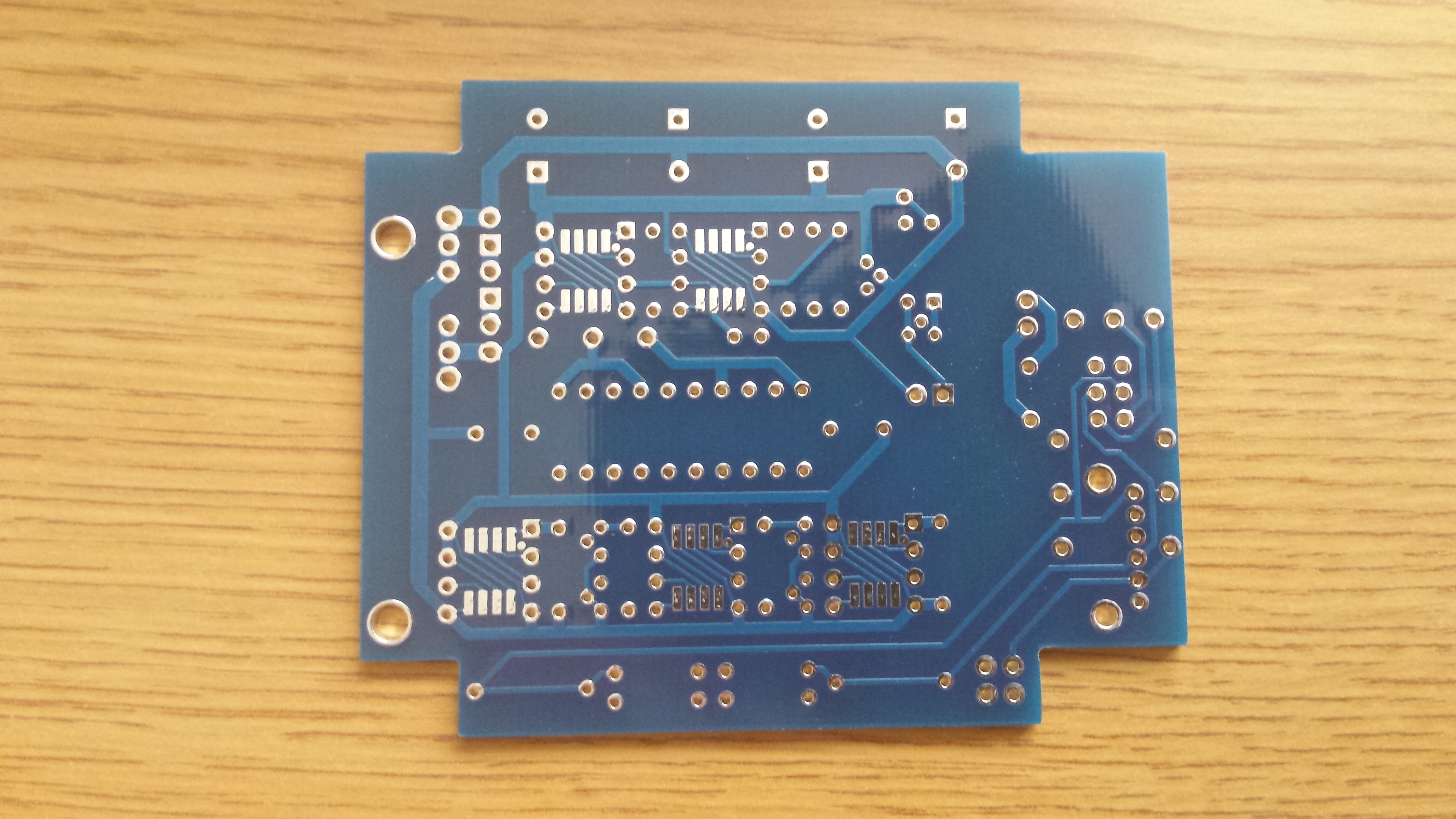
jumped buffer input to R7 (see pic to confirm i did this right)
I think it would have been simpler to just jump from pin 3 to 6 on each BUF SO-8 footprint, but buzzing it out on a bare board here says the pins you chose instead do also connect to the same locations.
Your use of bare wires for jumpers is a worry. You have to be very careful that they're not touching anything. Where I have to jump over exposed metal, I prefer to use insulated wire for jumpers, stripping it at the tips only.
A much bigger problem is how messy that soldering job is. Carbonized flux can be conductive, flux can trap conductive debris, and flux can conceal solder bridges. Even if it ends up not helping your immediate symptom, a good cleaning will at least add a touch of pride to the build.
- LED1 hole damaged so soldered direct to RLED
Have you watched
my soldering videos?
Unless your battery supply is going to be something marginal like 4 x AAA NiMH, that's not enough voltage to charge the battery. The
charge controller section of the docs should have made this clear.
That doesn't explain your present problems, but it's a risk of problems down the road. There is a
whole section of the docs on choosing a power supply for the amp, which your design choices seem to ignore.
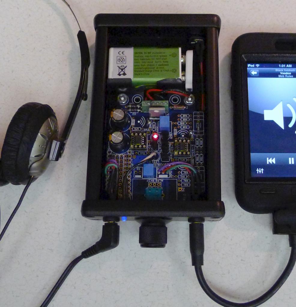
connected to the WALL molex 2 pin connector
That's not what your pictures show. The orange/white pair is connected to BATT.
Why are you using Molex connectors but soldering directly to them, anyway? You should be doing it one way or the other: hard-wire it or use connectors. If the orange/white pair is just for testing, I'd still make up a female Molex KK adapter. If you continue doing electronics, you may reuse that adapter later.
why is there a V drop when it is off???
D1 and
IC1.
When the ALPs is switched ON, the voltage at the WALL molex reads 8.06V
That means you're either using an unregulated power supply or it's too weak for the job. I highly doubt the latter, unless you've shorted something. The existing
troubleshooting guide tells you how to test the board's current draw, which will tell you if your board is drawing too much power for your wall wart.
In attempting to "check the voltages at all of the DIP-8 chips’ supply pins relative to input ground (IG)...should be about half the PS voltage..." I find that all pads for both opamps (not yet installed) read 0V except pin 5 for one and pin 6 for the other, which read 8.57V
I'm guessing this is due to your R1G hack. It appears you've misread the board labeling for the
scratchpad area, thinking the two long strips are IG. The docs make this clearer: there are only two IG pads in the scratchpad area. Using them for R1G is a bad idea. Just piggyback the two resistors on the existing R1G pads: solder one in place, then solder the other on top.


")
