the Pimeta-V2 thread
Oct 16, 2011 at 1:05 PM Post #376 of 651


Quote:
Hi,
 
In case you're interested, you can indeed build a Pimeta v2 handheld amp with the following features:
- Serpac H65 enclosure
- Li-Ion cell pack 14.8V 0.75Ah with protection circuit
- Integrated modified Linkwitz Crossfeed circuit
- Integrated Bass Boost and Volume Boost circuit
- Integrated battery level control circuit with bi-color led
 
For some of you this may be a bit over-engineered, but to me it was a good exercise.  The amp sounds brilliantly and qualitatively excellent, and the cells last for well over 10 hours.  As a proof, see the following pics.
 

Lots of cables for the filters and boosters, but eventually it will fit.  On the bottom see the bass/volume booster circuit as a piggi-back board to the R4 pins.


The 4 circuits all connected.  The Linkwitz circuit required the big caps to be soldered horizontally, while one of the C4 Wima caps had to be moved to the scratchpad area.
 

On the bottom of the pic see the battery control circuit, which goes as a vertical piggi-back board onto the sratchpad area.
 

All fits precisely into the enclosure.  The Li-Ion pack has been R&D'ed for this purpose - newest technology you can build these days.
 

Finally, the enclosure can be closed and the product is finished... happy listening!
 
Cheers.


those are full pack of pure awesomeness!!
 
i wanted to try to plant the the crossfeed before, but it's just too troublesome, plus, i want the amp to sound as pure as possible. now i prefer my pimeta than my previous iqube and balanced RSA Protector
biggrin.gif


Dec 26, 2011 at 4:25 PM Post #377 of 651
I've been trying to figure out how to run the pimeta from a dual supply.  I have 2 12v sla batteries
that I connect in series to run an amp for my speakers.  For some reason I only recently used
the batteries in series to power my pimeta.  Everything worked fine and I tried to find
information on using the 2 batteries as a dual supply.  I have 3 pimeta's that I built over a year
ago to play with seeing how different parts and configurations affected the sound.  Two of the pimeta's
have buffers and one is bufferless.
 
Now for the bad news.  I've tried to mod the 2 pimetas with buffers to run with a dual supply and failed.
Hopefully I haven't ruined them, but if I have it's not the end of the world.  I knew the risks of trying this
without coming to these forums and making sure what I was doing was correct.  On one pimeta all I
removed was the tle2426 and on the other I removed everything in the ground channel and the tle2426.
I connect the V+ from one battery and the V- from the other battery to + and - power connections on the
pimeta.  This is exactly the same as how I connect them to the pimeta with the batteries in series.  To
create ground I connect the positive and negative terminals on the batteries and run a wire out from this
connection to the pimeta.  I connect this ground wire to the IG on the scratchpad.  When I apply power
to either pimeta the buffers get burning hot very quickly, in fact I worry I've destroyed the buffers.  I've taken
some quick power measurements from pin 4 and pin 8 on OPALR.  On pin 4 I got -12.33 and pin 8 was 11.61.
 
Something is not right here and I have no idea what could be wrong.  Any help would be appreciated.
If I haven't been clear enough with my description then I'll be happy to provide more information.
 
Dec 26, 2011 at 5:48 PM Post #378 of 651
The PIMETA is not designed to be run from a dual supply.
You would be better off using a different amp designed to
be run from a dual supply.
 
If you really want to modify one, you will need to remove
all the ground channel components and jumper IG to OG.
Then you can use the center tap of your batteries as ground.
 
Jan 16, 2012 at 5:37 AM Post #379 of 651
Hi,
 
I've been trying to solve this problem by myself but I can't figure it out.. Could someone help me!
 
My problem is when I'm trying to run my pimeta from a 18v power supply, the leds won't light on. The op-amps and buffers are still unpopulated.
There are also a S1 shorting connector and jumper between ol and rblim pads which does not show in those pictures.
 
Pics:


EDIT: Problem solved.. LED1 was dead so I replaced it and jumpered LED2. Now everything should work.
 
 
Feb 12, 2012 at 2:52 PM Post #380 of 651


Quote:
Hi,
 
In case you're interested, you can indeed build a Pimeta v2 handheld amp with the following features:
- Serpac H65 enclosure
- Li-Ion cell pack 14.8V 0.75Ah with protection circuit
- Integrated modified Linkwitz Crossfeed circuit
- Integrated Bass Boost and Volume Boost circuit
- Integrated battery level control circuit with bi-color led
 
For some of you this may be a bit over-engineered, but to me it was a good exercise.  The amp sounds brilliantly and qualitatively excellent, and the cells last for well over 10 hours.  As a proof, see the following pics.
 

Lots of cables for the filters and boosters, but eventually it will fit.  On the bottom see the bass/volume booster circuit as a piggi-back board to the R4 pins.


The 4 circuits all connected.  The Linkwitz circuit required the big caps to be soldered horizontally, while one of the C4 Wima caps had to be moved to the scratchpad area.
 

On the bottom of the pic see the battery control circuit, which goes as a vertical piggi-back board onto the sratchpad area.
 

All fits precisely into the enclosure.  The Li-Ion pack has been R&D'ed for this purpose - newest technology you can build these days.
 

Finally, the enclosure can be closed and the product is finished... happy listening!
 
Cheers.

 
Wow,  Great job mfuerst. That's a lot of components to pack in such a small space.
Is that Lion battery control circuit board a commercial product, or did you design if yourself?


Feb 21, 2012 at 1:37 PM Post #381 of 651
Im an electronic engineering student. And for my electrical fab class i wanted to make a pimeta v2 headphone amplifier. one problem i was coming up with was finding the pcbs? does anyone know where i can get the circuit boards for this project. cause tangetsoft has a great parts guide but no link for the boards.
 
 
Mar 5, 2012 at 1:18 PM Post #383 of 651
I have a question about resistor values used in the pimeta.  After I failed to get my pimeta running from a dual supply I decided to go in another direction.  I'm using R1 and R2 as a voltage divider to drop the incoming audio signal around 30 decibels and from there I adjust volume digitally with foobar.  I've been using this setup for about a week and I'm really happy with how this is working out.  The only thing that is bothering me is the values I used for R1 and R2 are really low and I was wondering if R1 right and left can differ from R1 ground and R4 ground.  If I read the documentation correctly  these values are supposed the same.  Here are the values I'm currently using in my unity gain pimeta.
R1   6.49K
R2  220R
R3  empty
R4  6.49K
R5  shorted
R6  empty
R1G  6.49K
R4G  6.49K
 
My source is a gamma 1 which has 3ohm output impedance, so I think my current values are ok.  I have resistors on hand to change R1 right/left and R2 to higher values.  I could change R1 to 49.9K and R2 to 1.6K while leaving R1G/R4G at 6.49K so my source would see a higher input impedance from my amp.  Would I benefit from this change or should  I be ok with the current resistor values?
 
 
Mar 5, 2012 at 4:55 PM Post #384 of 651
If you're not using a volume pot on the PIMETA board and you're using JFET-input op-amps, you can put aside your input resistance worries. You might improve distortion a tiny bit by balancing the input resistances, but it probably isn't worth bothering about. It's more a thing we do because we can in the standard configuration.
 
Mar 6, 2012 at 1:16 PM Post #385 of 651
Thanks tangent.  I'm going to change R1 and R2 to higher values.  Hopefully I'll have the amp all cased up by the end of the weekend.  Its going into a translucent grey serpac H65.
 
Mar 8, 2012 at 2:18 AM Post #386 of 651
 
My PIMETA2 is broke -- please help!
 
Not meant to excuse myself of SNAFUs or responsibility -- nor do I claim any great DIY skill :wink: … but …(along with several other “DIY” amps and mods), I’ve successfully built both a PPA2 and this now-“broke” Pimeta2 -- they all have worked pretty much from the get go… up to and including several interim tweaks and op-amp rolls. And, for well over a year, my Pimeta2 has survived near-everyday use (including gazillions of the ever-inconvenient 9v NiMH changes). Again, all w/o incident. Until now … my “indestructible” Pimeta2 has crashed, big time, and I have not been able to troubleshoot it for a week -- literally 20+ hrs of hair-pulling and still no luck.
 
How it all started (?? best guess!) and where stuff stands …
 
After rolling in a new op-amp, I turned the Pimeta2 on and heard a loud pop over my IEMs. 
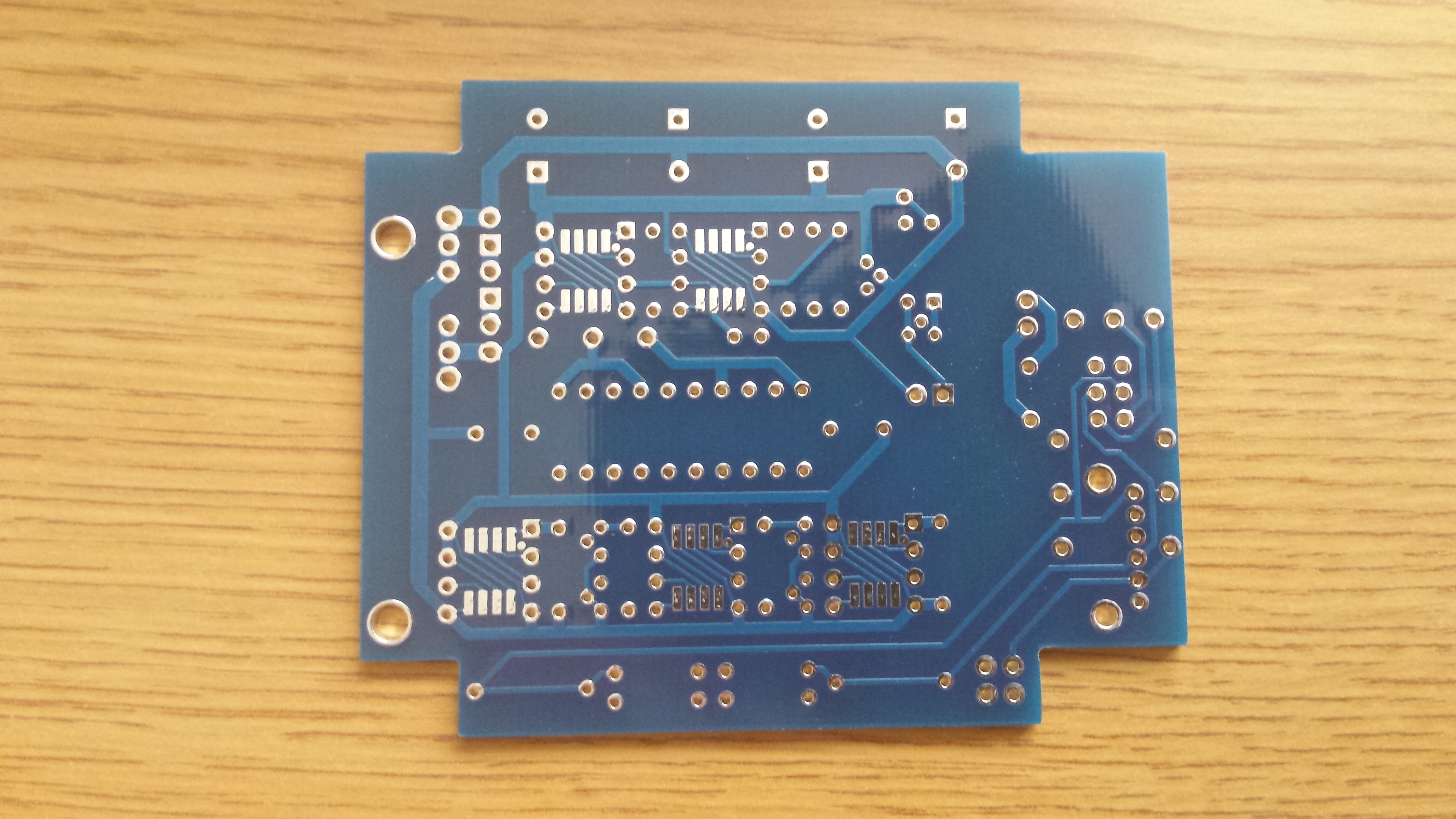
Cause: I did not seat the opamp properly into the 8-DIP plug-in socket -- so  I seated it correctly and turned on the amp. Sounds fine again but now LED2 is not lit (LED2 is one of two the class-A-biasing LEDs from Tangent’s schematic; I’ve always used both LED1 and LED2, and they are mounted on the front panel for easily visibility). Troubleshooting, I found that as I was inserting the opamp, I had broken one of the pins on Q2 (2N3904) [I use a SOIC-to-DIP BrownDog adptr and that’s hard to squeeze in w/o bending some of nearby components, like Q2.] Anyway, I replaced Q2, and the LED was restored … but now, I heard a loud pwr-on thump in the L ch only (which is now also dead); R-ch sounds fine and no pwr-on thump).
 
After a bit of checking, I noticed that the opamp (AD8620 or 8066) was getting VERY warm after about 5 sec. I moved the opamp to a breadboard and attempted “piecemeal” troubleshooting. The opamp draws 54mA (!!) when the V_out1 (Pin 1 for L-channel on dual-ch opamps) is normally connected to the L-ch ckt in front of it -- this includes the feedback loop, PREBUF, 100-ohm R, and the LMH6321 buffer.
 
If I disconnect the opamp’s V_out1 pin (L-ch), it draws a mere 8mA .If I swap output pins (dual opamp's pin 7 now feeds the L-ch ckt in front, I get the same 54mA draw -- this will make the opamp v. warm in a few secs). Feeding ONLY the R-ch ckt (L-ch open in front of opamp) with either V_out pin results in normal 8mA draw.
 
Note: opamp V_out (1 or 7, i.e., whichever is feeding L-ch ckt in front of it) has V = 2.8vdc. The one that feeds R-ch is normal (few mV)
 
I haven’t checked the LM6321 buffer’s current draw -- FWIW, it runs cool. And they do have built-in "OVERVOLTAGE PROTECTION" per National's datasheet. Just in case, I also replaced it (L-ch only). No diff (for all I know, this buffer could have blown again by whatever else is messing up the L-ch). I also replaced Q3L (2N3904, the L-ch op-amp class-A bias trans).
 
I checked the output of the buffer (the ‘phones O/P jack) -- and L-ch turns on with (and remains at) a whopping 2.6 volts DC offset (no wonder I heard that pop-thump)!! R-ch is normal (3-4mV). All this with NO audio/music signal at input -- i.e., running idle. Soundwise, R-ch sounds fine, while L-ch is "dead"/broke/whatever.
 
Shorts in the L-ch ckt ahead of the opamp output? None I could find with a decent DMM (Fluke 87). Alas, my o’scope is itself dead so I can’t do detailed troubleshooting.
 
Power suppl. -- which is TLE2426-based with 9v batt (default) -- seems to be fine -- so, all powered opamps/buffers are getting proper +/- 1/2 the supply volts.
 
Other notes:
- I've almost never use passive "protection" (on any amp :wink: -- for the Pimeta2, that means C1 is bypassed (jumpered). BUT ... I do use output-current-limiting resistors, R11 (3k-ohm), for all buffers.
- Ground channel seems to be fine (this is a deduction based on the fact that R-ch seems to be good).
 
Questions:
With the L/R-ch opamp(s) REMOVED, but with the buffers connected (in normal circuit), why do I get large DC offset at output for BOTH channels?
L-ch: 2.6V (as noted above); R-ch: 160mV.
If there is no input, the buffers should not output any voltage (other than a few mV idle, of course). Or am I missing something here?
 
My brain is mush and my head is bald from all the hair-pulling! Please help -- thanks!
 
[BTW: after that initial thump, which my IE-8s survived, I switched to a pair of junk cans -- they seem to be able to handle the 2.5V DC offset. This is how I’m able to test for music/signal and distortion]
 
EDIT: Problem solved (or isolated) somewhat ...  but WHY?
 
Okay, I noted above that I replaced Q3L (the L-ch class-A bias trans.). Honest to dog I replaced it with another 2N3904 -- and I did. Yet when I removed it (just a few mins ago), all returned to behaving "normal" (at least WRT basic metrics: DC o/p offset is normal, quiet pwr-on/off, no pops or crackly volume, etc) ... except that topologically I have a 2N3904 Q3R for R-ch, and the rest of the class-A transistors (and all the related LEDs and resistors) all in situ  (i.e., nothing else removed, bypassed or jumpered). What just happened? What is STILL happening: I installed another NEW 2N3904 and the problem returns again! (dunno if it's same batch as orig 2N3904 -- the one that worked in the Pimeta2 orig. built 2 yrs ago -- the one that I replaced a few days ago). I tried another putatively higher-quality NPN (Toshiba 2SC2240, and accounted for its pin diffs) ... but same problem when installed in the Q3L footprint. Yes ... I checked all traces -- with Q3L removed -- for shorts or opens. All's normal. At least as far as I can test. I haven't tweaked the bias trimpot because (I assume) Q3R is functioning normally???
 
 
Mar 8, 2012 at 4:43 PM Post #387 of 651
The last required bits for my PIMETA2 showed up today, so I can finally start building. Here's the plan:
 
  1. Hammond 1455 enclosure  with custom laser-cut front and back panels from Ponoko NZ
  2. Integrated Alien USB DAC, powered from the amp.
  3. AD8620/8610 SMD opamps (soldering direct to board because I forgot to order the browndog adapters)
  4. 10xAAA NiMH cells for a 12V supply. I was going to go with 9.6V, but then realised I needed V+/2 to be at least 5V for the DAC.
  5. Moving the trickle charger to another board (or prototyping area), so that the battery can be fully isolated from the amp while charging from a switchmode supply. I'm doing this to avoid any potential ground-loop problems via USB.
  6. Battery level meter using a LM3914 in dot mode with a 3 red / 7 green LED bar graph. (Depends how low I can get the current draw - this might end up having a push-button to check battery level).
  7. a switched 3.5mm socket between the DAC and amp to act as a line-in for analog sources.
 
For C1 I have some 470nF WIMA MKS4 polyesters that fit the board perfectly, or some 220nF polyprops that overhang and will need to have a leg bent back under the board to reach the pad. Hopefully I'm not about to spark a religious war here, but is it worth going with the polyprop in this case, or the polyester with the lower corner frequency?
 
Mar 8, 2012 at 4:53 PM Post #388 of 651
Quote:
after that initial thump, which my IE-8s survived, I switched to a pair of junk cans -- they seem to be able to handle the 2.5V DC offset. This is how I’m able to test for music/signal and distortion

 
You should have been testing only for DC offset, from the start. It is not a sufficient test, but you would have seen the problem without risking your expensive IEMs or your junk cans. Nothing you've reported about how the problem sounds tells us anything more than a high DC offset measurement would have.
 
Maybe you're annoyed now, thinking I'm armchair quarterbacking. But, a DC offset test is one of the standard testing steps. When you rolled that op-amp, you should have gone back through that test sequence. Plugging cans in is four paragraphs down the sequence, and it recommends starting with the cheapies.
 
Quote:
With the L/R-ch opamp(s) REMOVED, but with the buffers connected (in normal circuit), why do I get large DC offset at output for BOTH channels?

 
Because you've broken the feedback loop.
 
The class A biasing circuitry is dragging the input of each buffer to V-, so the output will go as close to V- as it can get, without the op-amp there to fight against the bias.
 
With Q3L out, you would still expect a high DC offset between OL and OG with the op-amp out because then the input of BUFL is left floating, so it can be pushed about by RFI and electrostatic fields in the room.
 
Bottom line, there's no point in testing what's happening at OL and OR when there is no op-amp plugged in.
 
Quote:
What just happened?

 
It is indeed a mystery why Q3L is behaving differently from Q3R.
 
Since the two transistors should do the same thing at all times when under the same forces (and they are, in the idle amp tests) and you have exonerated Q3L, that leaves the op-amp.
 
So: put the original op-amp back in. Does the DC offset symptom go away? If so, the amp probably sounds fine now, too. (As good as it can sound through cheap cans, because you're not going to test with expensive IEMs first again, are you now? Of course not. You've already learned that lesson. 
redface.gif
)
 
Quote:
(I assume) Q3R is functioning normally???

 
It's not hard to test. With the op-amp removed, put your meter on the milliamps scale and stick it between V+ and pin 7 on the op-amp socket. You should get 3 mA or less, and it should change as you adjust the trim pot.
 
If that gives believable results, you can then try measuring between op-amp pin 1 and V+, while Q3L is installed. There is some risk to the meter here, as we haven't absolutely proven that the left channel bias path actually behaves the same as the right. You might want to start with the meter on the amps scale, if you have one. (Typically 10 A.) Even in the worst case, the meter should survive if there is a dead short down this path. Then once you get a believably small reading, you can switch to the milliamps scale.
 
Mar 8, 2012 at 5:06 PM Post #389 of 651
Quote:
  1. Integrated Alien USB DAC, powered from the amp....I needed V+/2 to be at least 5V for the DAC.

 
I don't know anything about that DAC, but you'll want to check that its output is AC coupled. It won't work otherwise.
 
 
Quote:
  1. Battery level meter using a LM3914 in dot mode with a 3 red / 7 green LED bar graph. (Depends how low I can get the current draw - this might end up having a push-button to check battery level)

 
If you end up going with the pushbutton method, I think it would be neat to use the chip in bar mode but feed it through an RC filter with a time constant of half a second or so. You would then see it "fill up" the bar over the course of a few seconds, rapidly at first, then leveling off at the true value. It should look cool.
 
 
Quote:
is it worth going with the polyprop in this case, or the polyester with the lower corner frequency?

 
I'd go with the polypropylene cap if it's not a box type. If it is, the legs probably aren't ductile enough to withstand the sharp bend, and are likely break. If not during the assembly attempt, then shortly after due to vibration.
 
If you don't need the cap to create an AC-coupled situation between the DAC and PIMETA, I'd short C1, because you already effectively have an input cap.
 
Mar 8, 2012 at 5:56 PM Post #390 of 651

 
Quote:
I don't know anything about that DAC, but you'll want to check that its output is AC coupled. It won't work otherwise.

 
It's a PCM2702-based design. Site here. It's normally AC-coupled with 47uF electrolytics (for space reasons I think - the board is tiny). The analog section runs on 5V, so the caps are always forward-biased by around 2.5V. I figured that it's probably best to use the coupling caps on the PIMETA, so I'm taking the signal from the capacitor + pads on the DAC. The DAC draws power for its analog section from V+ and GND on the amp (it buffers the ground via a BUF634 so as not to adversely affect the ground level in the amp). Some people have reported problems due to a voltage offset between the input of the buf634 and the output ground of the DAC. (I saw this when testing the DAC using a voltage divider for the ground level). The solution seems to be to reference IL and IR against the amp ground instead of IG coming from the DAC.


If you end up going with the pushbutton method, I think it would be neat to use the chip in bar mode but feed it through an RC filter with a time constant of half a second or so. You would then see it "fill up" the bar over the course of a few seconds, rapidly at first, then leveling off at the true value. It should look cool.

 
Good idea, will try it out tonight... Another potential mod described on the data sheet is to do a simple PWM on the voltage signal so that the brightness of the last LED indicates the fractional portion of the voltage.
 
Quote:
I'd go with the polypropylene cap if it's not a box type. If it is, the legs probably aren't ductile enough to withstand the sharp bend, and are likely break. If not during the assembly attempt, then shortly after due to vibration.
 
If you don't need the cap to create an AC-coupled situation between the DAC and PIMETA, I'd short C1, because you already effectively have an input cap.

 
It is a box cap, but the leads do not exit the cap body flush with the board (the bottom is slightly inset). Do you think it'd be OK if the lead had more of a radiused bend? The way the caps overhang the corner notches of the board means that I've got the thickness of the board to work with when bending the pins. (I can take a photo when I get home, but basically one pin would be normal through-hole on one end and the other would bend back under the board to meet the SMT pad. Would this introduce problems via the inductance of the longer lead, or is that irrelevant at audio frequencies?
 
edit: spelling
 

Users who are viewing this thread

Back
Top