


K3cT
Headphoneus Supremus
- Joined
- Apr 1, 2007
- Posts
- 2,751
- Likes
- 397
Quote:
I think it's thermal paste.
That's possible although I'm fairly sure that's not the normal way of using it. Besides, the location seems inconsistent from one build to another.
I think it's thermal paste.
The solder is not good, the comments I posted about the yellow and red joints were actually made by a professional in the field and the white blob is http://en.wikipedia.org/wiki/Thermal_grease
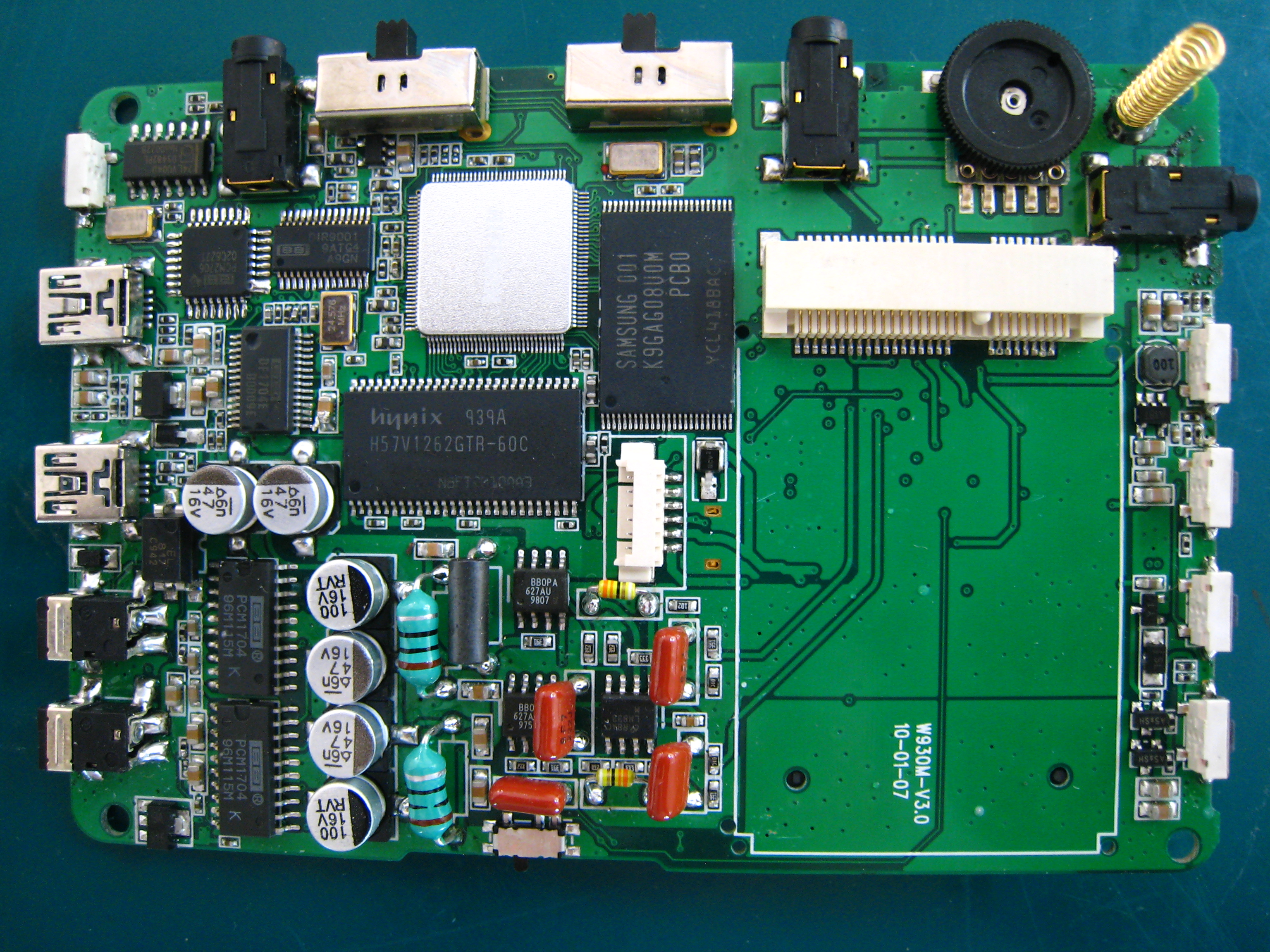
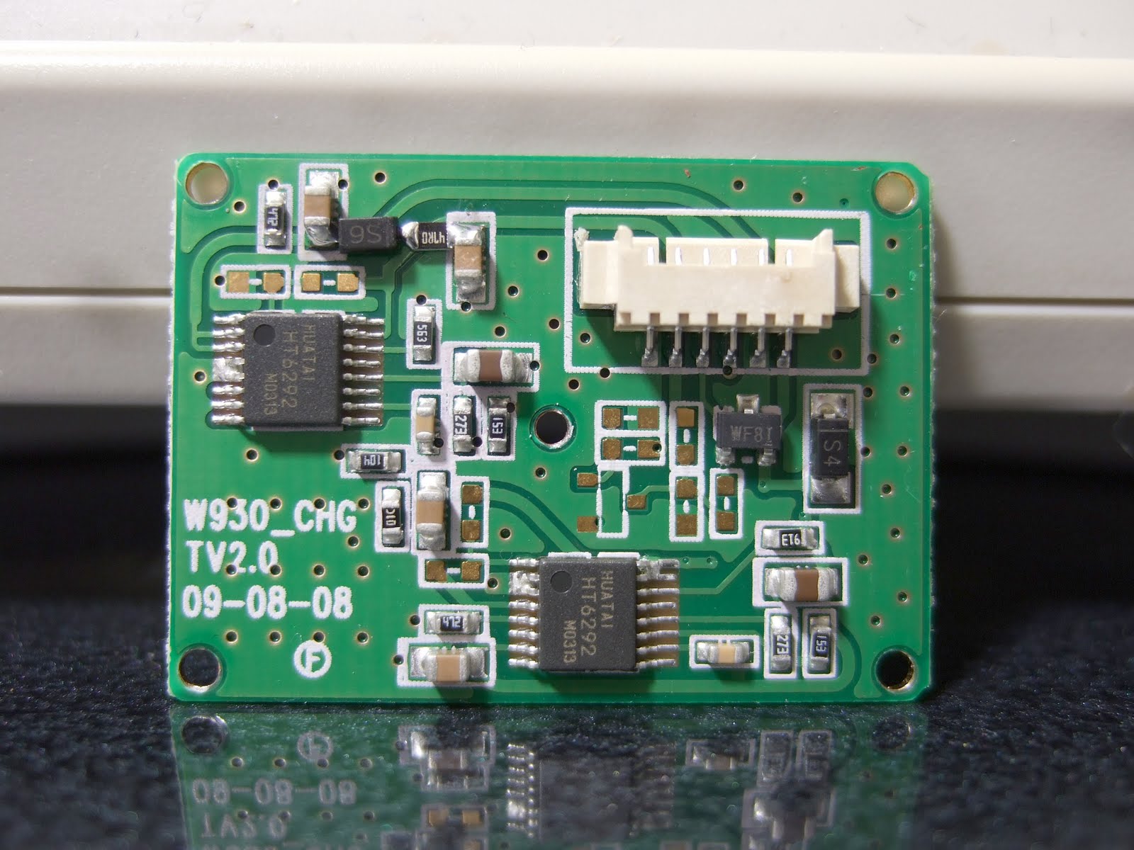
Pictures of the internals ...
I'm so happy you posted that link for all to see the soldering and spew on the pcb board, I think this speaks volumes without having to say much other than my 12 year old son can solder cleaner ... this finally shows the poor quality of solder joints, judge for yourself. Is this a DAP that is worth $800.00 and the size of that power supply reminds me of what I used in the mid to late 80's, there are more pictures as I only posted a few from your link JohnFerrier, http://light-widely.blogspot.com/2009/10/hifiman-hm-801.html You really need to use the link to see close up the poor quality, huddler just resizes the pictures too small ...
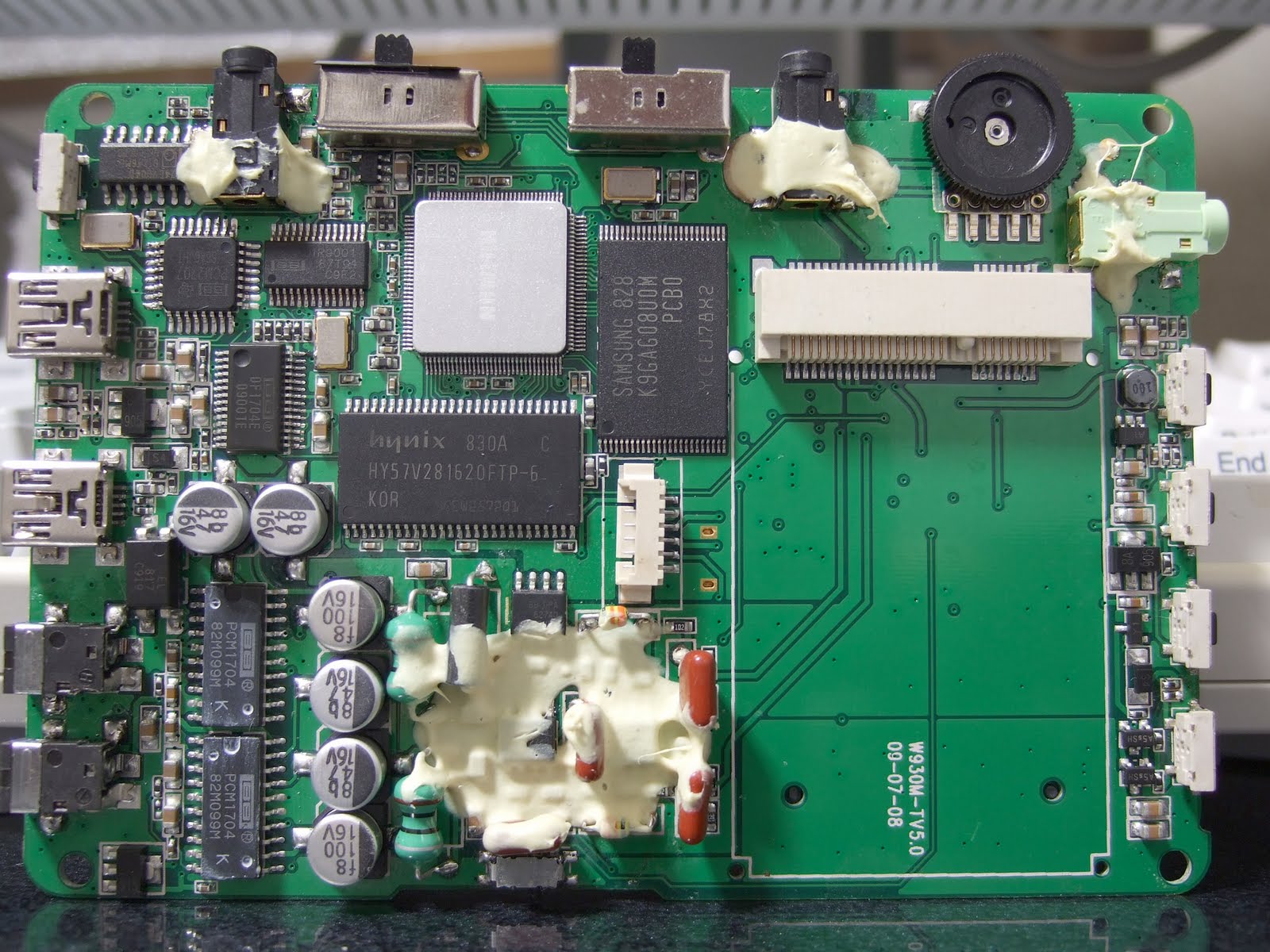
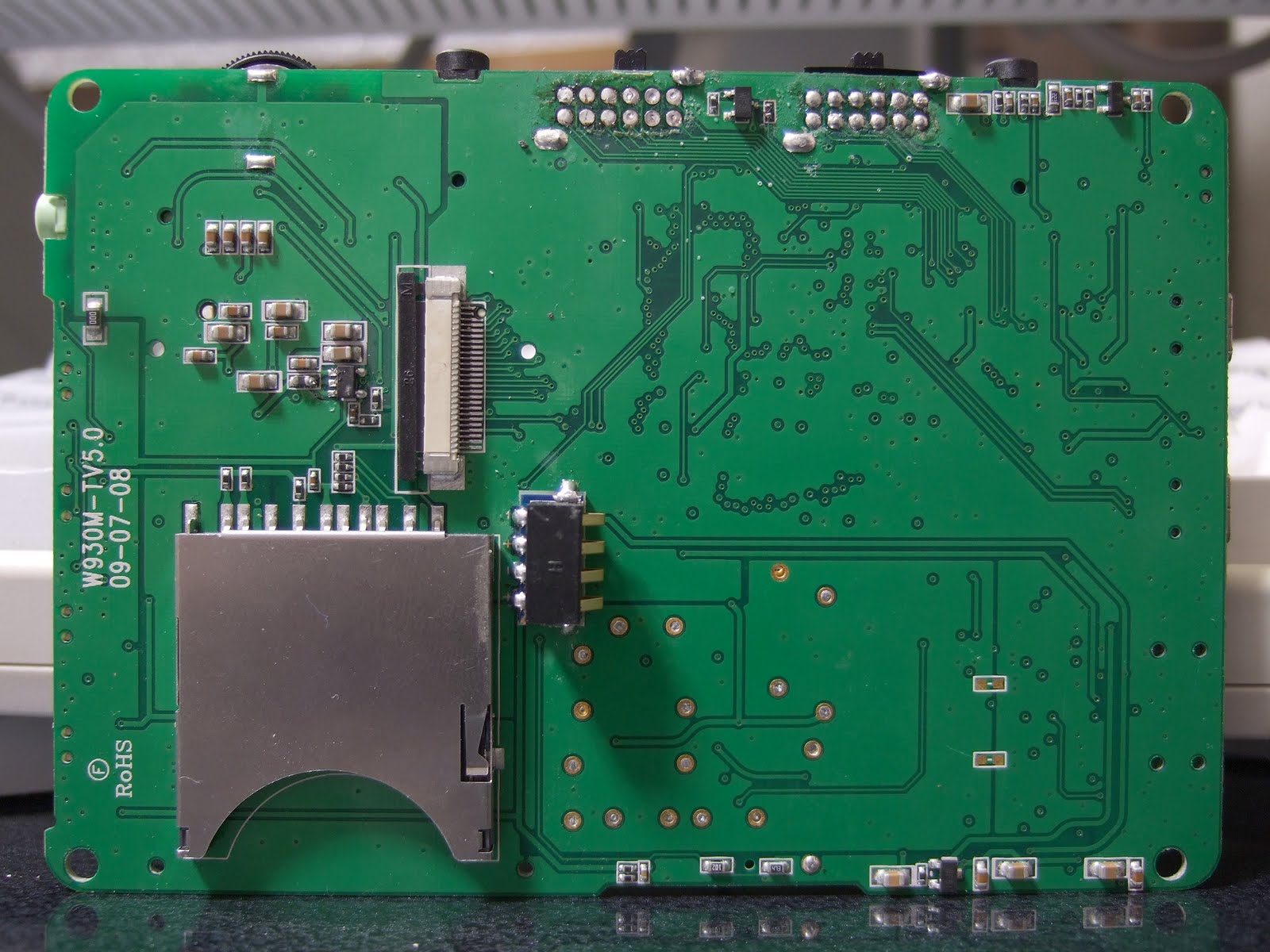
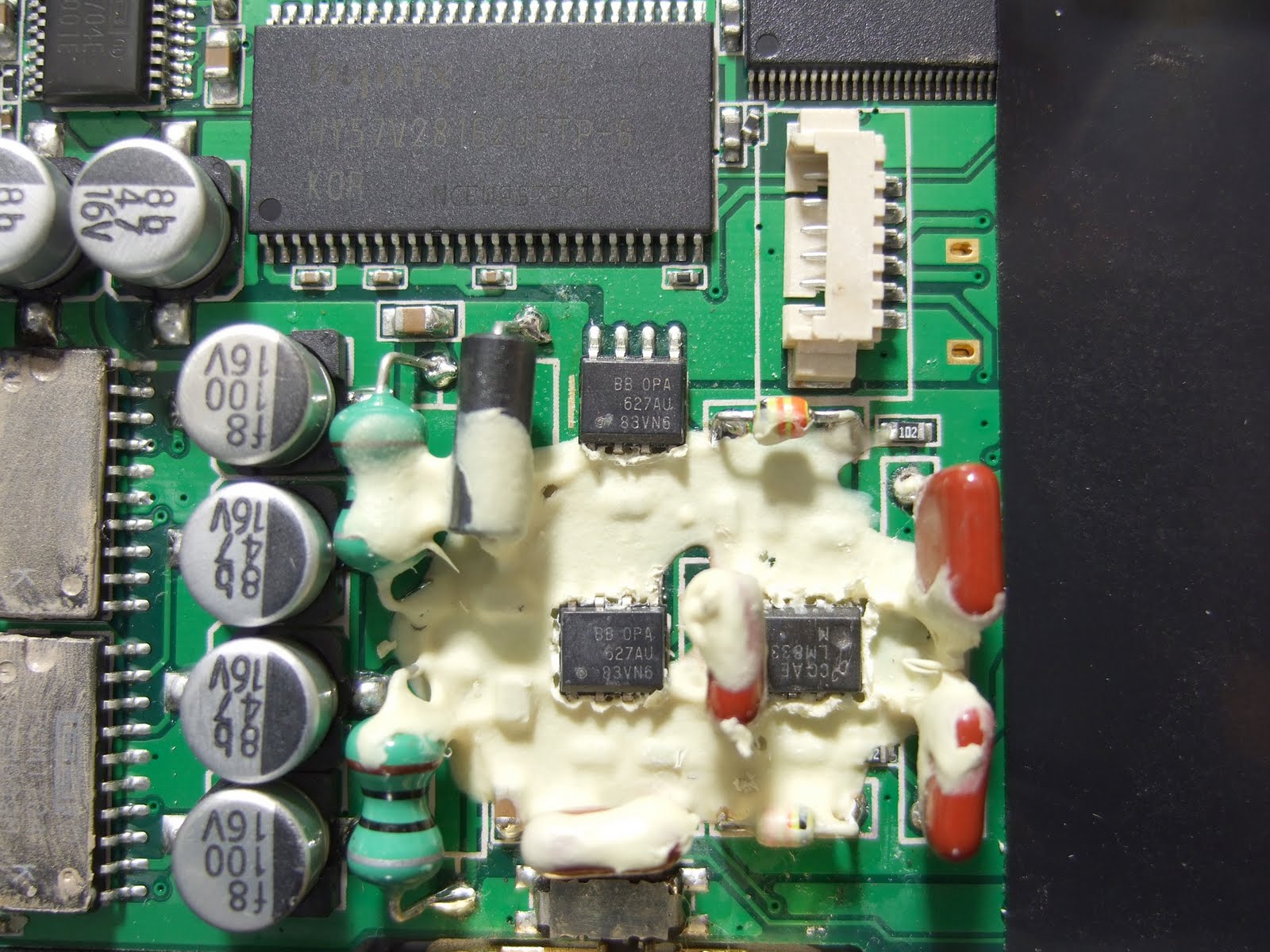
For an $800.00 DAP, the pcb not to be set up via on a soldering robot is a joke rather than hand soldered by kids in China. Any reputable company would use soldering robots, if the manufacturer did it might look something like the Sansa Clip inside. And don’t come back with the argument that it’s hand made, it's just stock electronic parts pieced together by unskilled hands. The yellow is questionable, red is so bad that it should be rejected and the uppermost red circle is the scariest with the huge wad of solder around it that tiny resistor almost touches the memory chip. Seriously, as a commercial product there is no excuse for mediocrity, especially at that price this is totally unacceptable.
Beyond the graphs, if you add up lack of batter life, build quality, UI, sound quality all that matters when coming to a conclusion. Not to mention that wonderful 60 day warranty it’s a clogged artery just waiting to happen
here's the link so you can see close up: http://i41.tinypic.com/2wcmvz8.jpg

You don’t need schematics to tell if a solder joint is good or not, but hey if you like the craftsmanship enjoy …
Actually I am looking at it now and I'm having difficulties finding the exact soldering faults at some of the circles.
Luckily for you the blatantly bad solder is circled in bright colours making it easy to see for those such as yourself without the knowledge of what good solder jobs look like.

As long as data is able to travel through the circuit board and it's safe to handle, it's fine.
Luckily for you the blatantly bad solder is circled in bright colours making it easy to see for those such as yourself without the knowledge of what good solder jobs look like.
.gif)
Wooo... straight to the baseless generalizations, very amusing. I have a feeling that you yourself do not know what bad solders look like.
Anyway I'm done here. Please carry on with your hate campaign.
I'm just saying you're exaggerating your claim of bad soldering. Though I agree the white blobs look really icky.
High resistance and dry joints are acceptable then are they?
")
Even a software guy can see the big blobs and cold soldier points and ...

