


KT88
500+ Head-Fier
- Joined
- Nov 7, 2004
- Posts
- 948
- Likes
- 26
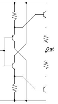
A very cool implementation of a virtual-GND circuit.
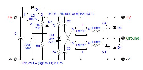
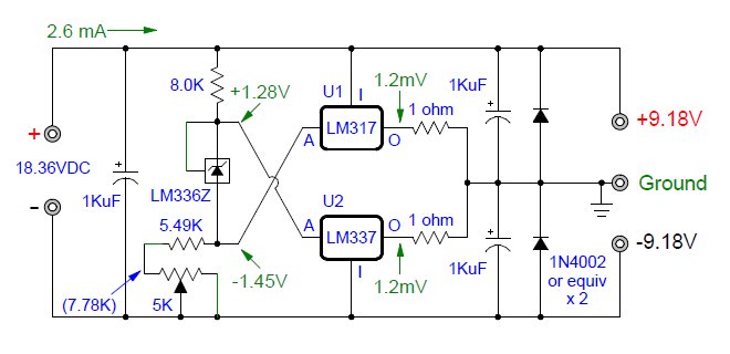
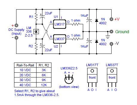
As for the latest circuit in goldpoint's post, I see a couple of issues with it:
A. The zener current is only about 0.8mA, and it probably need at least a couple of mA to operate with the nominal voltage across it.
B. The zener voltage can be in the +-5% range, and the internal reference of the LM317 and LM337 can be 1.2V-1.3V which is a +-4% compared to the 1.25V nominal value. That means there could be a difference of up to 225mV between the zener voltage and the reference of the LM317+LM337. So that's up to 225mV across the resistors at the output which yields a current of <=225/(2*R)mA (assuming there's sufficient current in the zener to keep its voltage in specs - no enough current will force a higher voltage across these resistors and therefore more wasted current). The biggest issue is what would happen if the zener voltage is high, and both regulators have a low reference so that Vzener>(Vref317+|Vref337|) - this would make the LM317 output voltage be lower than that of the LM337, and the circuit won't work as its supposed to work. So the designer/builder must make sure this doesn't happen.
Some current at the output is actually a good thing, since the LM317 requires up to 12mA of current at the output to maintain regulation (this is the maximum value, nominal value is about 3.5mA). However since the current will depend on the exact value of the reference voltages it can't be trusted.
C. A different way to look at this circuit is as a push-pull op-amp capable of sourcing/sinking >1.5A (at least that one of ways I see it") ). The LM317 sources current, while the LM337 sinks current. As long as you maintain a minimum current at the output of both regulators its basically a class-A/AB buffer with the zener diode trying to compensate for the offset of ~1.25V from the A to O pins of the regulators (1.25V for each regulator). So perhaps instead of trying to use voltage regulators and compensate for the voltage variations which yields great variations in the DC current, it would be best to implement a class-A or AB (probably better) follower with the input generated using a simple resistive voltage divider between the rails as its usually done. This is what most op-amp circuits do, so using an op-amp can work fine, its just a matter of finding one with sufficient current drive capability, and low cross-over distortion - most op-amps now-days actually keep the output transistors operating with a small current at all times, but this current is usually very small to minimize power consumption, and therefore some cross-over distortion can still be noticed.
). The LM317 sources current, while the LM337 sinks current. As long as you maintain a minimum current at the output of both regulators its basically a class-A/AB buffer with the zener diode trying to compensate for the offset of ~1.25V from the A to O pins of the regulators (1.25V for each regulator). So perhaps instead of trying to use voltage regulators and compensate for the voltage variations which yields great variations in the DC current, it would be best to implement a class-A or AB (probably better) follower with the input generated using a simple resistive voltage divider between the rails as its usually done. This is what most op-amp circuits do, so using an op-amp can work fine, its just a matter of finding one with sufficient current drive capability, and low cross-over distortion - most op-amps now-days actually keep the output transistors operating with a small current at all times, but this current is usually very small to minimize power consumption, and therefore some cross-over distortion can still be noticed.
D. Another point I want to mention is that I think the virtual-GND circuit should be tailored to the amplifier in use. Some amplifiers have a very different PSRR between the two supplies, so in some cases it might be better to implement a "simple" virtual-GND circuit that regulates the virtual-GND with respect to one supply rail or the other (which one would depend on the amplifier used).
As for the latest circuit in goldpoint's post, I see a couple of issues with it:
A. The zener current is only about 0.8mA, and it probably need at least a couple of mA to operate with the nominal voltage across it.
B. The zener voltage can be in the +-5% range, and the internal reference of the LM317 and LM337 can be 1.2V-1.3V which is a +-4% compared to the 1.25V nominal value. That means there could be a difference of up to 225mV between the zener voltage and the reference of the LM317+LM337. So that's up to 225mV across the resistors at the output which yields a current of <=225/(2*R)mA (assuming there's sufficient current in the zener to keep its voltage in specs - no enough current will force a higher voltage across these resistors and therefore more wasted current). The biggest issue is what would happen if the zener voltage is high, and both regulators have a low reference so that Vzener>(Vref317+|Vref337|) - this would make the LM317 output voltage be lower than that of the LM337, and the circuit won't work as its supposed to work. So the designer/builder must make sure this doesn't happen.
Some current at the output is actually a good thing, since the LM317 requires up to 12mA of current at the output to maintain regulation (this is the maximum value, nominal value is about 3.5mA). However since the current will depend on the exact value of the reference voltages it can't be trusted.
C. A different way to look at this circuit is as a push-pull op-amp capable of sourcing/sinking >1.5A (at least that one of ways I see it
). The LM317 sources current, while the LM337 sinks current. As long as you maintain a minimum current at the output of both regulators its basically a class-A/AB buffer with the zener diode trying to compensate for the offset of ~1.25V from the A to O pins of the regulators (1.25V for each regulator). So perhaps instead of trying to use voltage regulators and compensate for the voltage variations which yields great variations in the DC current, it would be best to implement a class-A or AB (probably better) follower with the input generated using a simple resistive voltage divider between the rails as its usually done. This is what most op-amp circuits do, so using an op-amp can work fine, its just a matter of finding one with sufficient current drive capability, and low cross-over distortion - most op-amps now-days actually keep the output transistors operating with a small current at all times, but this current is usually very small to minimize power consumption, and therefore some cross-over distortion can still be noticed.D. Another point I want to mention is that I think the virtual-GND circuit should be tailored to the amplifier in use. Some amplifiers have a very different PSRR between the two supplies, so in some cases it might be better to implement a "simple" virtual-GND circuit that regulates the virtual-GND with respect to one supply rail or the other (which one would depend on the amplifier used).

