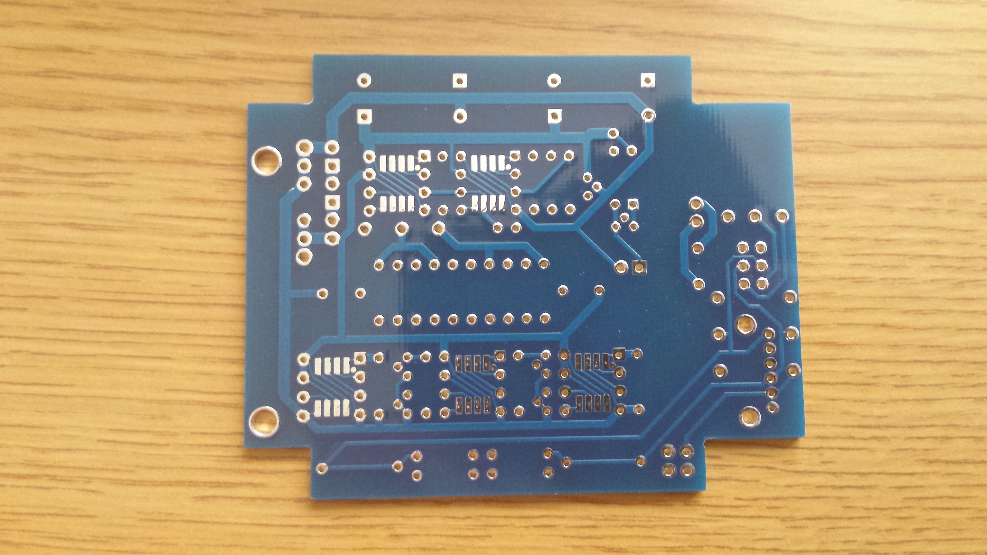
the Pimeta-V2 thread
May 10, 2010 at 7:01 PM Post #151 of 651
 
 
Quote:
in which one can find active circuits to pass a balanced signal into an unbalanced one, and vice-versa.

 
Why add yet another active stage when it's not necessary?


Quote:
Now I would like to keep balanced line through the pimeta, so I should pick up the signal, and have it re-balanced to an output.

 
Look into 4-channel amps.  You could probably use the PIMETA v2 scratchpad to build a fourth channel and hack the ground channel to be its mate.

 
Jun 3, 2010 at 8:10 PM Post #153 of 651
I've been working the last couple of days on a Pimeta v2. I've gotten it mostly put together, successfully tested the power supply, and gone on to the buffers. I soldered pin 1 of the first buffer to its pad, and then gently nudged one of the other pins with my iron. The chip simply fell off the board, pad and all.
 
I think the work that I have put into the amp has instantly been trashed. These are the only components that absolutely have to be surface mounted, and with no pad, there is no way to attach it. Correct?
 
I am going to get a drink.
 
Jun 3, 2010 at 8:23 PM Post #154 of 651
check the schematic... that pin is probably not used if it fell off that easily...  (Something similar happened to me on a Mini^3.)
 
Jun 13, 2010 at 4:01 AM Post #156 of 651
If I want 3 milliamps from biasing by using the stock values and don't want adjustability, do I solder RBLIM so that it "spans the switchable bias jumper pads" as shown in the step by step assembly guide, or do I solder it so that it spans all the way into the RBIAS slot too?
 
Jun 13, 2010 at 2:45 PM Post #157 of 651
Your question is answered at the bottom of the parts selection guide section on RBLIM: http://tangentsoft.net/audio/pimeta2/pguide.html#RBLIM  There's even a picture.
 
Jun 13, 2010 at 4:03 PM Post #158 of 651
Well I mean, that's what confuses me. So the assembly guide assumes that you'll be wanting to use an adjustable trim pot and the selection guide doesn't. I was just making sure is all.
 
Oh also, the schematic values for C3 says that it should be 470 uF but the part selection guide/list says and gives parts for .1uF. This also confuses me and I'm kind of wary of soldering any on since the values are so different.
 
I didn't want to bump the thread so edit: Thanks for fixing things! I appreciate the clarifications.
 
Aug 8, 2010 at 12:12 AM Post #160 of 651
 
Aw nuts!!  Just checked my DC offset. OG about 1mV; OR about 25mV; OL about..... 233mV!?*#%
Solder joints look good, nothing gets hot, everything else checks out. Using AD8066/8065. Battery
power (1 - 8.4V NiMH). Any ideas?
 
Oops! Just realized I don't have anything in C6G 'cuz I only ordered two cap's instead of three.
Maybe that' the problem with the ground channel.
 
Aug 8, 2010 at 9:35 PM Post #161 of 651
Yes, C6 is most definitely not optional.
 
Aug 9, 2010 at 9:23 PM Post #163 of 651
 
All is well. I replaced the L channel buffer, installed a 33pF C6G that I had and it's up and it's sounding great. Now I need to
order some 25V C2's as I'm measuring a little over 17V to the (16V) C2's I've got in there now when I connect
the 18V PS to charge the battery. The 25V cap's are 16mm tall, so I hope they'll fit.
 
Aug 9, 2010 at 11:46 PM Post #164 of 651
Good to hear it.
 
A cheaper way to fix the C2 problem would be to put another diode or two inline with the power supply's V+ line.
 
Also, be sure you're measuring at the caps, not at the power inlet pads on the board.  The existing on-board diode OR bridge will buy you a half a volt or so already.
 

Users who are viewing this thread

Back
Top