2 or 3 Channel, Single Ended Class "A" Design Thread

May 25, 2010 at 5:47 PM Post #32 of 87
On my large heat sink it changes very little.
If you design your amp to get really hot by using too
little heat sink, then you can expect the offset to shift
more. If you use enough heat sink so it feels warm
to the touch but not uncomfortably hot then offset
is more controlled. I will check one of my channels
for you and let you know the difference between hot and cold.
 
Quote:
How's the offset after warming up ?Does it change ?


May 25, 2010 at 6:37 PM Post #33 of 87
I adjusted one of the channels to 0 just after turning it on with
the heat sink at room temperature.
After 30 minutes of running so the heat sink about as warm
as it usually gets, I had +1.1 mV offset.

 
Quote:
How's the offset after warming up ?Does it change ?


May 25, 2010 at 7:25 PM Post #34 of 87
OK, after an hour I think it is as hot as it is going to get.
The heat sink is now about as warm as a cup of coffee
that is comfortable to drink. I have three channels running
at 152mA @ 20 volts mounted to this...
 
The channel I adjusted to 0 when cold is still at 1.1mV
The other channel, which doesn't even have an adjustment
is at -.8mV.
 
I think the reason my offset stays so small is that I match/adjust
the current source rather than the input bias.
 
I think I saw somewhere that anything less than 20mV offset
is considered safe...
 
May 31, 2010 at 9:51 AM Post #35 of 87
Here is the next version I am building.
I'll try and make this one look a little prettier too...
 
Current should be 140mA per channel.


May 31, 2010 at 7:13 PM Post #36 of 87
Hi, go for it (...but first consider re-labelling either the bottom left power connection or the left FET gate because they are both currently called ground!!!)
 
You might also benefit from small caps at each FET from drain to PSU ground.
 
 
I hope it works well, : )
 
May 31, 2010 at 8:13 PM Post #37 of 87
Ya, your right...I should rename it.
Thanks.
 
Quote:
Hi, go for it (...but first consider re-labelling either the bottom left power connection or the left FET gate because they are both currently called ground!!!)
 
You might also benefit from small caps at each FET from drain to PSU ground.
 
 
I hope it works well, : )


Jun 1, 2010 at 8:43 AM Post #38 of 87


Do you have this schematic in a better resolution where it can be read?  I think it is showing a servoed CCS on the top of the mofsets controlling DC offset that way.    This would give much better PSRR than the other solutions posted thus far.
 
 
Quote:
 
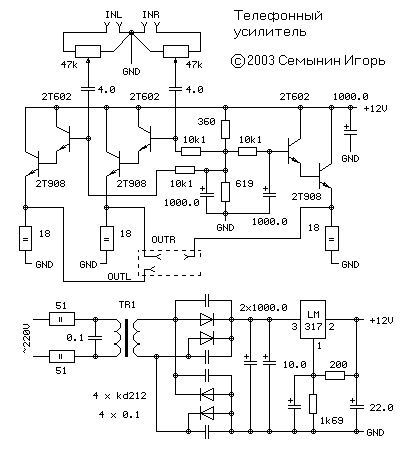
No. The bias is tuned for maximum transistor's linearity.
 
Such psu will be ok, but you will need C-R(or L)-C filter anyway. you may use a 7812 - it doesn't needed any extra resistors.
 
The simulation will not be correct because of simplified lm317 model.
 
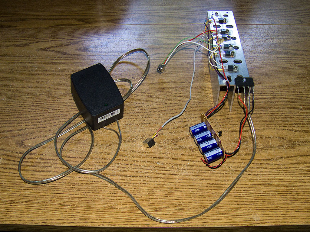
Here is one more intresting schematic.


Jun 1, 2010 at 10:55 AM Post #39 of 87


Quote:
Do you have this schematic in a better resolution where it can be read?  I think it is showing a servoed CCS on the top of the mofsets controlling DC offset that way.    This would give much better PSRR than the other solutions posted thus far.

Pdf file is here.
http://www.musatoffcv.narod.ru/Projects/HA-1/HA-1-sch.pdf
The image resolution was ok. You just need to click on it to see the larger image.
smile.gif

 
Jun 13, 2010 at 10:56 AM Post #42 of 87
Looks nice and simple!
I can't quite work out how C1 is working? Just passing positive rail noise to the junction of R1 and R2?
Is the gain simply  - R3 / R9 , or does R5 have to be factored in?
Should have a lot of PSRR!
 
Jun 13, 2010 at 2:12 PM Post #43 of 87
According to the designer, C1 reduces power supply hum
R3/R5 set both the gain and the bias. I'm not really sure what R9 is there
for...
 
Quote:
Looks nice and simple!
I can't quite work out how C1 is working? Just passing positive rail noise to the junction of R1 and R2?
Is the gain simply  - R3 / R9 , or does R5 have to be factored in?
Should have a lot of PSRR!


Jun 13, 2010 at 4:23 PM Post #45 of 87
R3 and R9 together form a kind of negativ feedback, I think.
Why don't you try this design with the same current source but a follower instead of this common source. Single-ended class A with no voltage gain ?
 

Users who are viewing this thread

Back
Top