


the power supply section in 002 is different from the 001.
regulator for incoming power: 001 has a linear voltage regulator to drop the incoming voltage to around 2.8V, if the input is much higher than it will generate heat to burn off excessive input power (Q15 gets hot). In the 002 the voltage regulation is done by a switch mode buck/boost chip, LTC3127, which takes whatever input voltage (supposedly anywhere from 1.8V to 5.5v is ok) and sends out regulated output voltage. It should have much higher efficiency than the linear regulator in the 001, so heat from this section of the circuit will not be a problem.
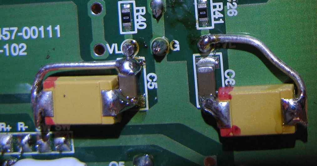
The step-up transformer in 002 is driven by a pair of SMD transistor (marked NAI, not sure what model # they are, looks very much like the Q11/Q12 transistors in the 001), these transistors are driven by two tiny three-lead SMD devices, with "FQ 17" marking. Reference designators are Q9/Q10 so I assume they are transistors of some sort. There is not much else. (the circuit in 001 is much more complicated, involves a LM358 and a 74HC14, plus 6 tiny transistors).
I will try to find out where the 002 transformer driver system gets the switching signal from. Maybe from one of the pins of LTC3127 (which is a switch mode device after all).
update:
-- looks like the LTC3127 is both used for incoming DC voltage regulation (PWM only, continuous mode) and the ripples at output is used as the trigger for the step-up transformer driving circuit.
-- the input range for the chip is 1.8v to 5.5v. (but I would stay between 3v and 5v; the sound started to fall apart when voltage got below 2.5v)
-- the circuitry seems to inject a fixed amount of power into the system, so current draw will go lower with higher supply voltage. My modded 002 ( opamps changed to Muses 8920, therefore consumes a little more power than a stock amp) draws about 600mA at 2.6v, but only 330mA at 4.5v.
-- the circuit in the 002 sets a input average current limit of 620mA.
regulator for incoming power: 001 has a linear voltage regulator to drop the incoming voltage to around 2.8V, if the input is much higher than it will generate heat to burn off excessive input power (Q15 gets hot). In the 002 the voltage regulation is done by a switch mode buck/boost chip, LTC3127, which takes whatever input voltage (supposedly anywhere from 1.8V to 5.5v is ok) and sends out regulated output voltage. It should have much higher efficiency than the linear regulator in the 001, so heat from this section of the circuit will not be a problem.
The step-up transformer in 002 is driven by a pair of SMD transistor (marked NAI, not sure what model # they are, looks very much like the Q11/Q12 transistors in the 001), these transistors are driven by two tiny three-lead SMD devices, with "FQ 17" marking. Reference designators are Q9/Q10 so I assume they are transistors of some sort. There is not much else. (the circuit in 001 is much more complicated, involves a LM358 and a 74HC14, plus 6 tiny transistors).
I will try to find out where the 002 transformer driver system gets the switching signal from. Maybe from one of the pins of LTC3127 (which is a switch mode device after all).
update:
-- looks like the LTC3127 is both used for incoming DC voltage regulation (PWM only, continuous mode) and the ripples at output is used as the trigger for the step-up transformer driving circuit.
-- the input range for the chip is 1.8v to 5.5v. (but I would stay between 3v and 5v; the sound started to fall apart when voltage got below 2.5v)
-- the circuitry seems to inject a fixed amount of power into the system, so current draw will go lower with higher supply voltage. My modded 002 ( opamps changed to Muses 8920, therefore consumes a little more power than a stock amp) draws about 600mA at 2.6v, but only 330mA at 4.5v.
-- the circuit in the 002 sets a input average current limit of 620mA.
