


joneeboi
Headphoneus Supremus
- Joined
- Jul 7, 2006
- Posts
- 1,919
- Likes
- 21
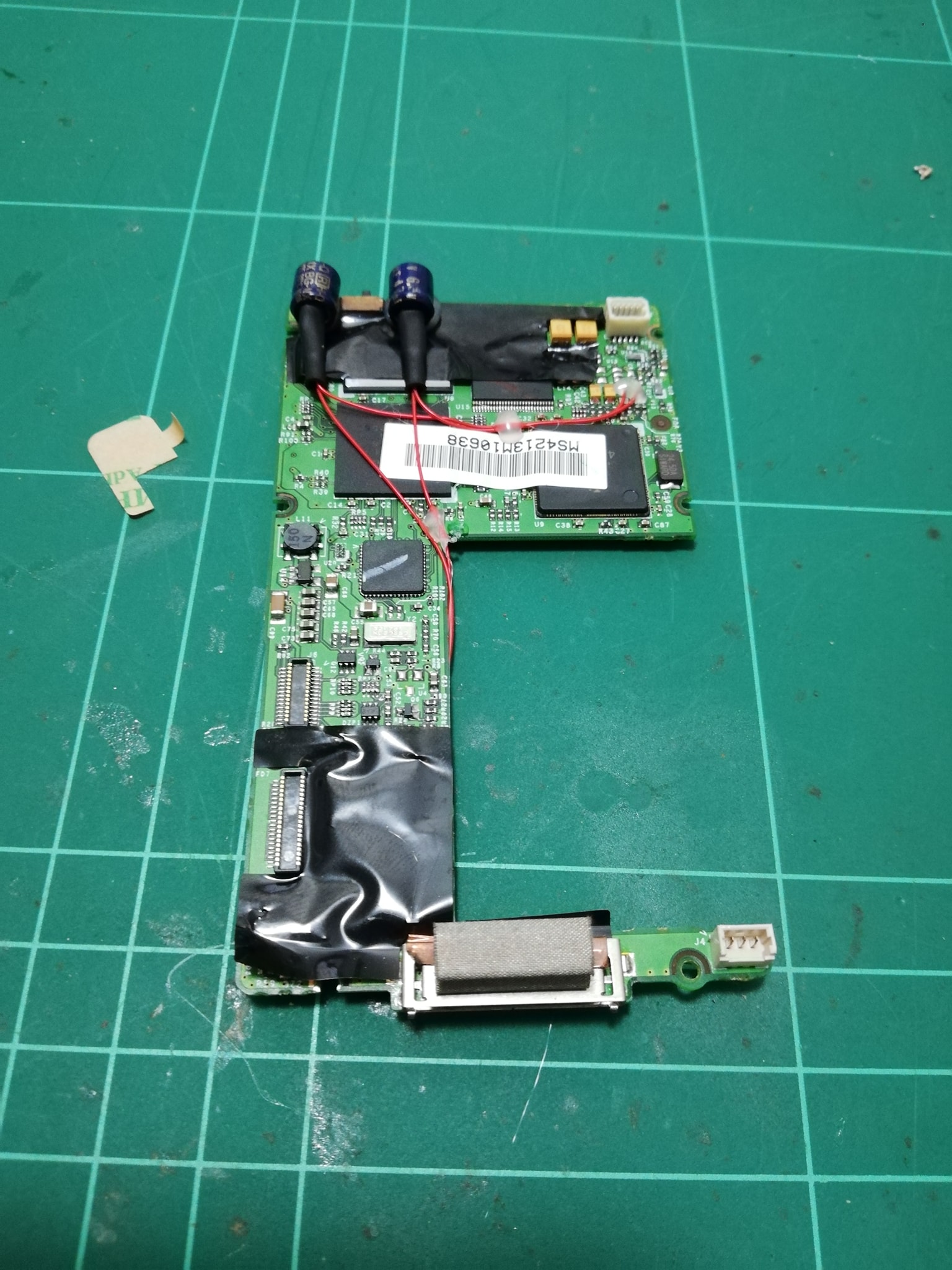
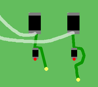
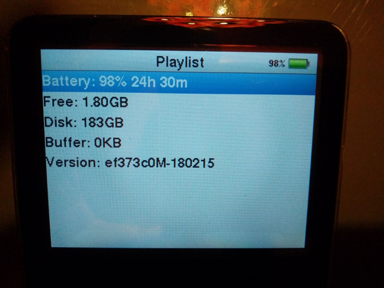
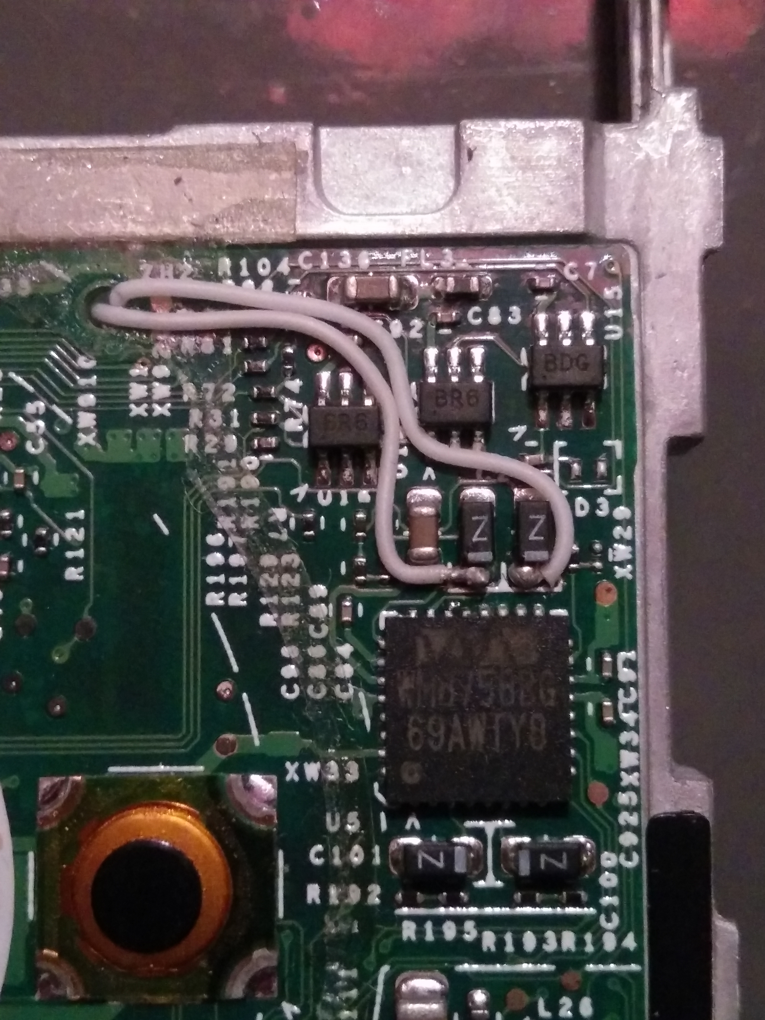
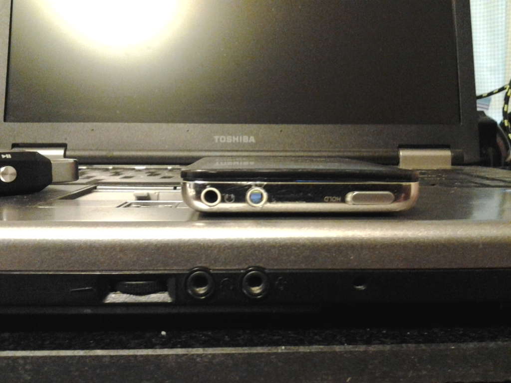
There is a lot that I have to work on, but I'm publishing it as is for now since I've been procrastinating this for years. I'll work on adding stuff like guides on how to open each device, but for now, there should be enough to go on to do your own diyMod.
https://www.instructables.com/id/DiyMod/
https://www.instructables.com/id/DiyMod/

")
