pupDAC Step-by-Step Build Thread
Nov 17, 2012 at 9:30 AM Thread Starter Post #1 of 359

tomb

Member of the Trade: Beezar.com
Joined
Mar 1, 2006
Posts
10,890
Likes
1,049
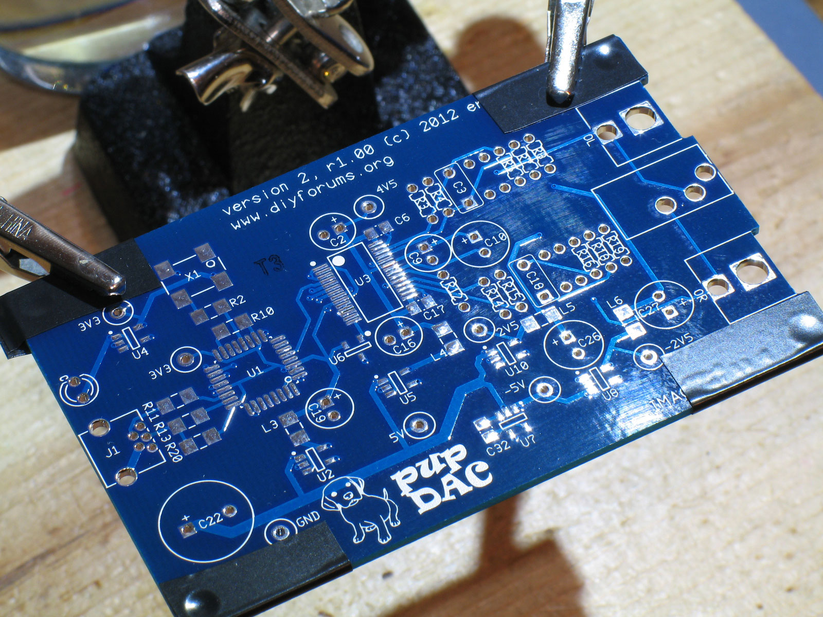
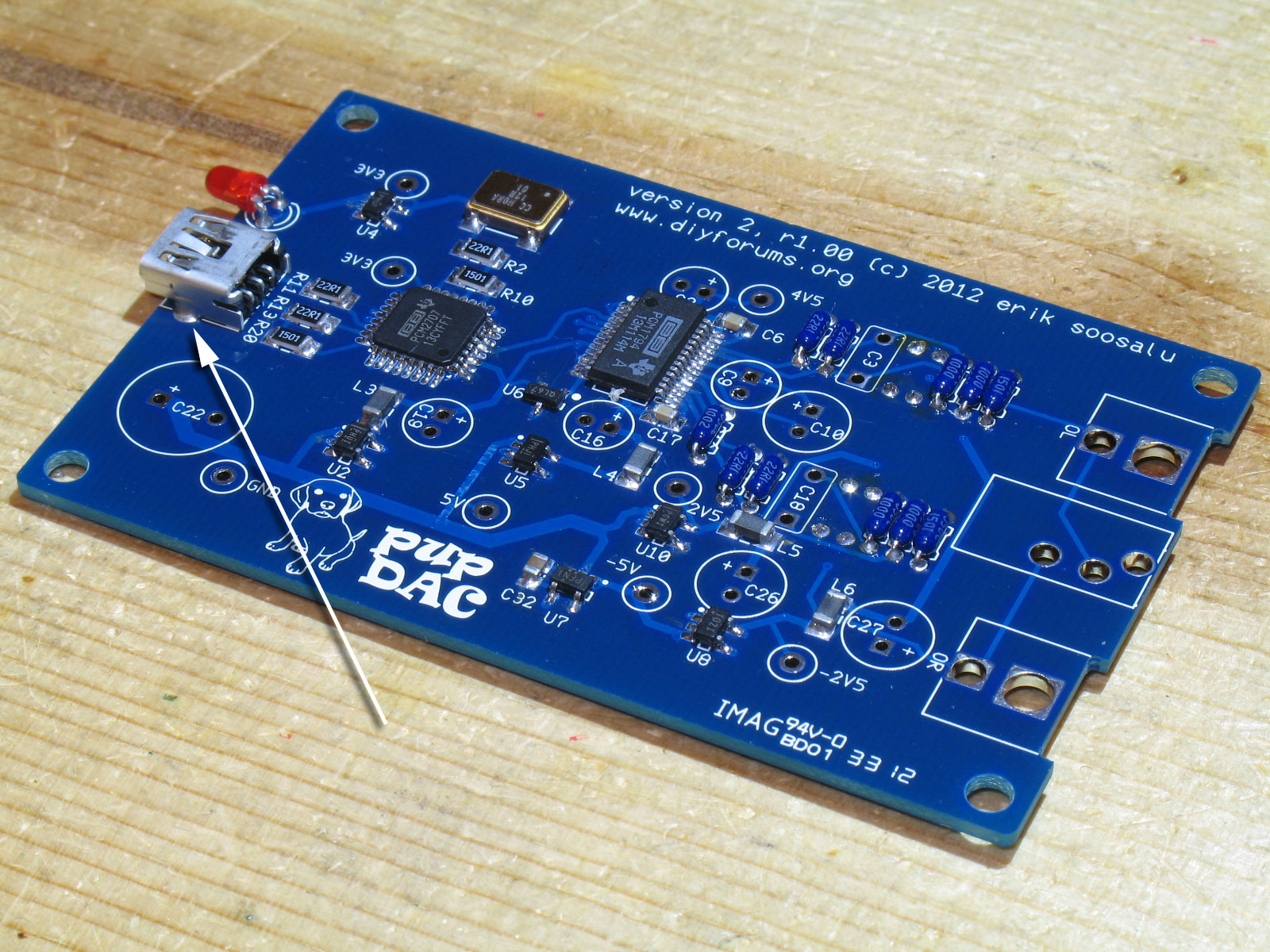
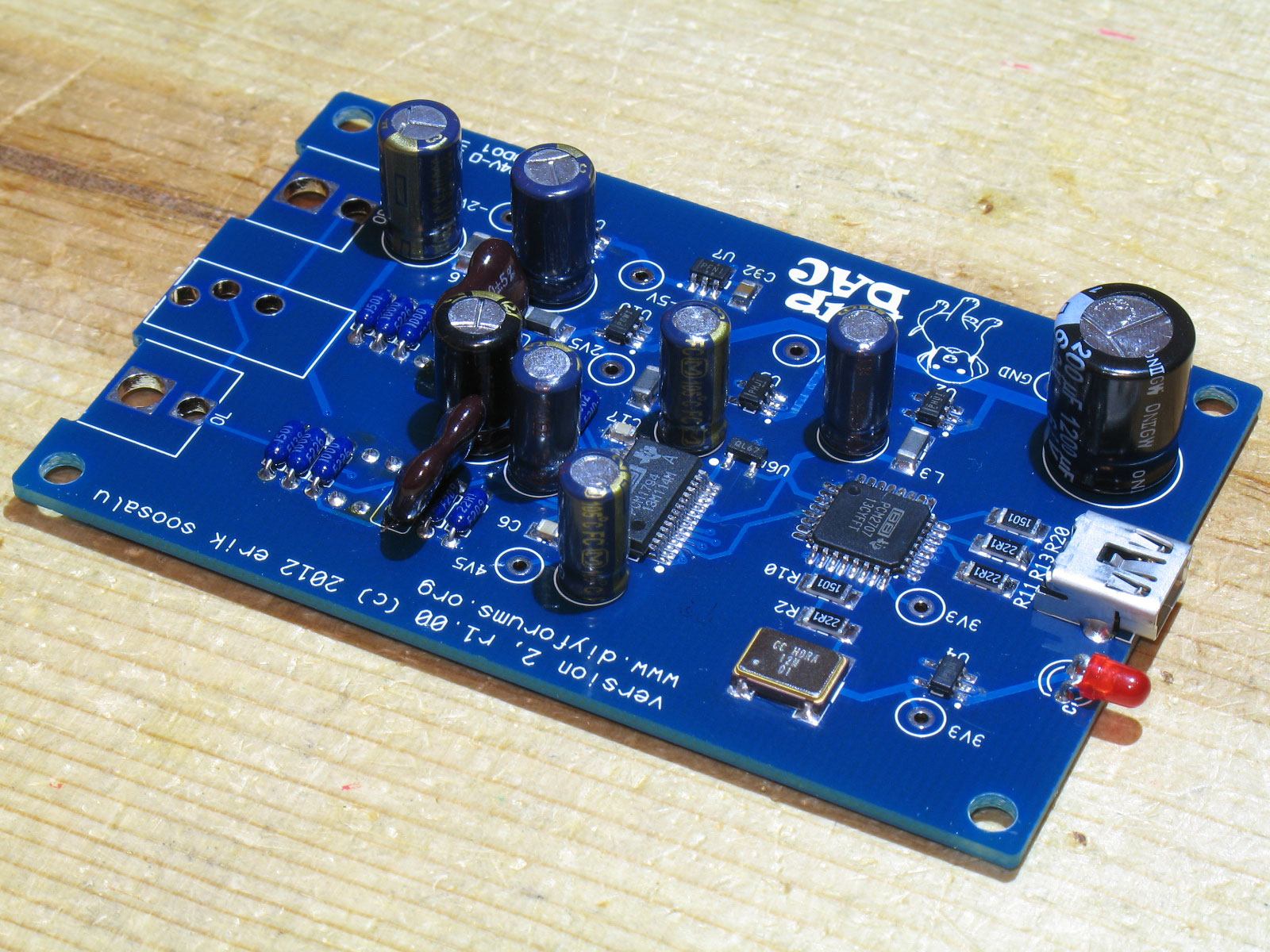
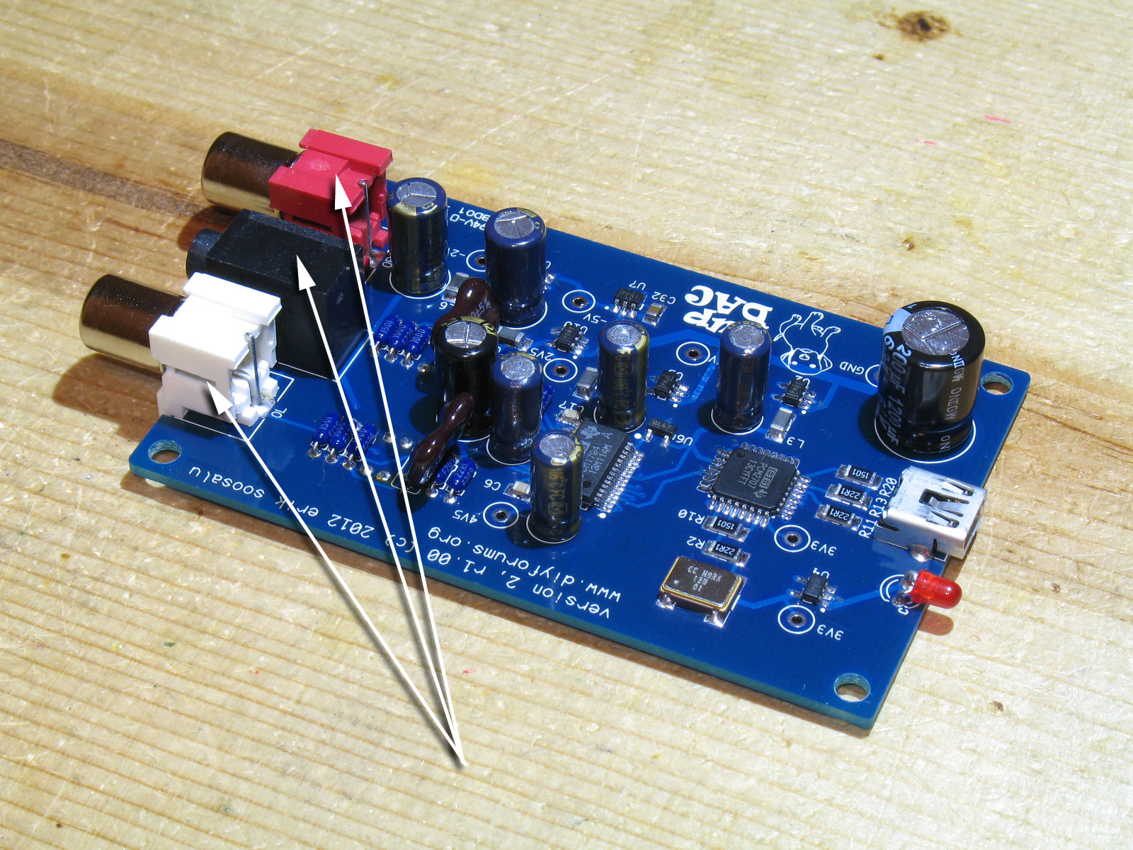
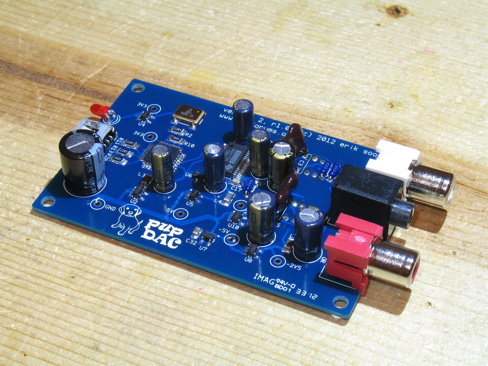
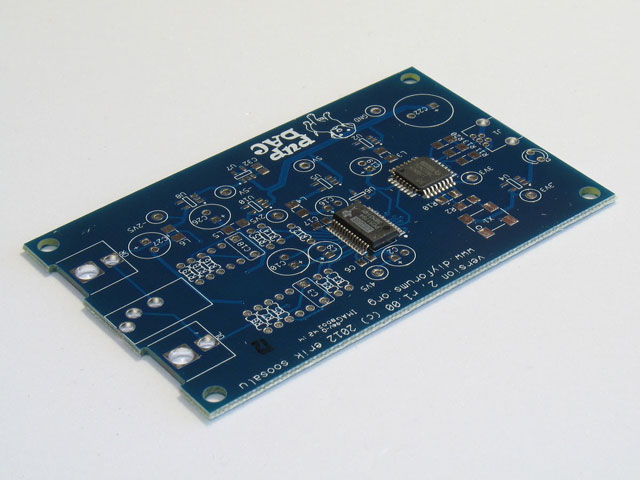
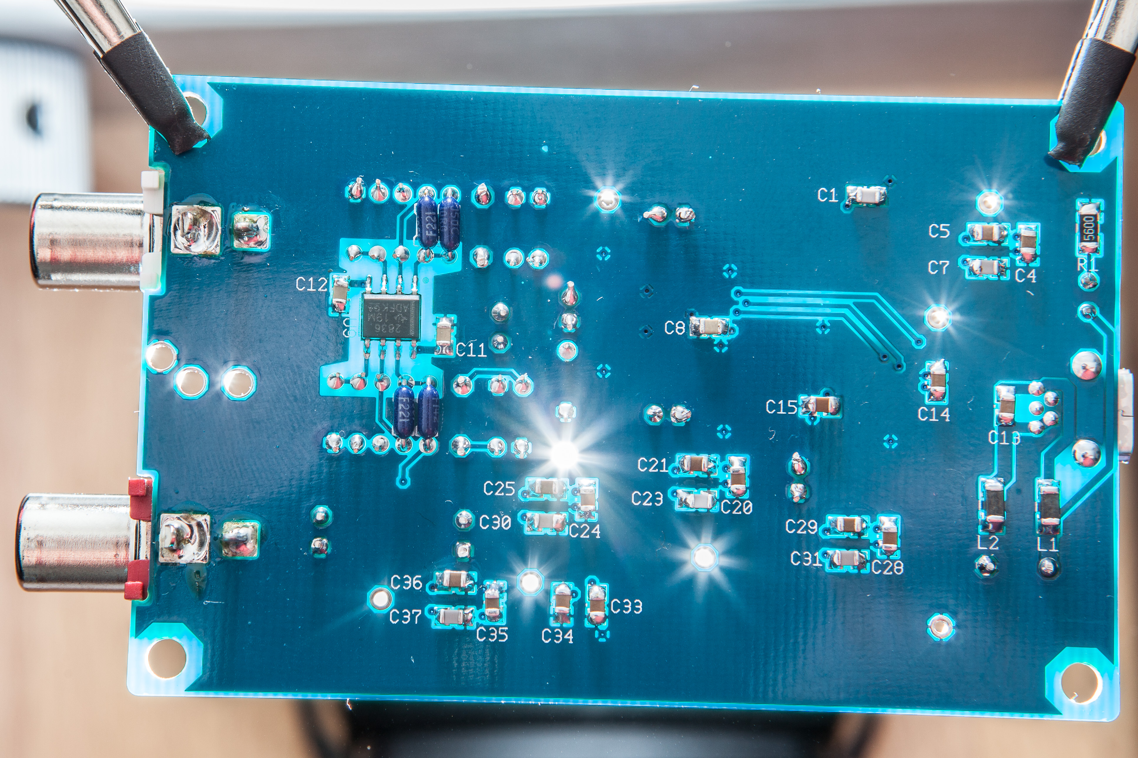
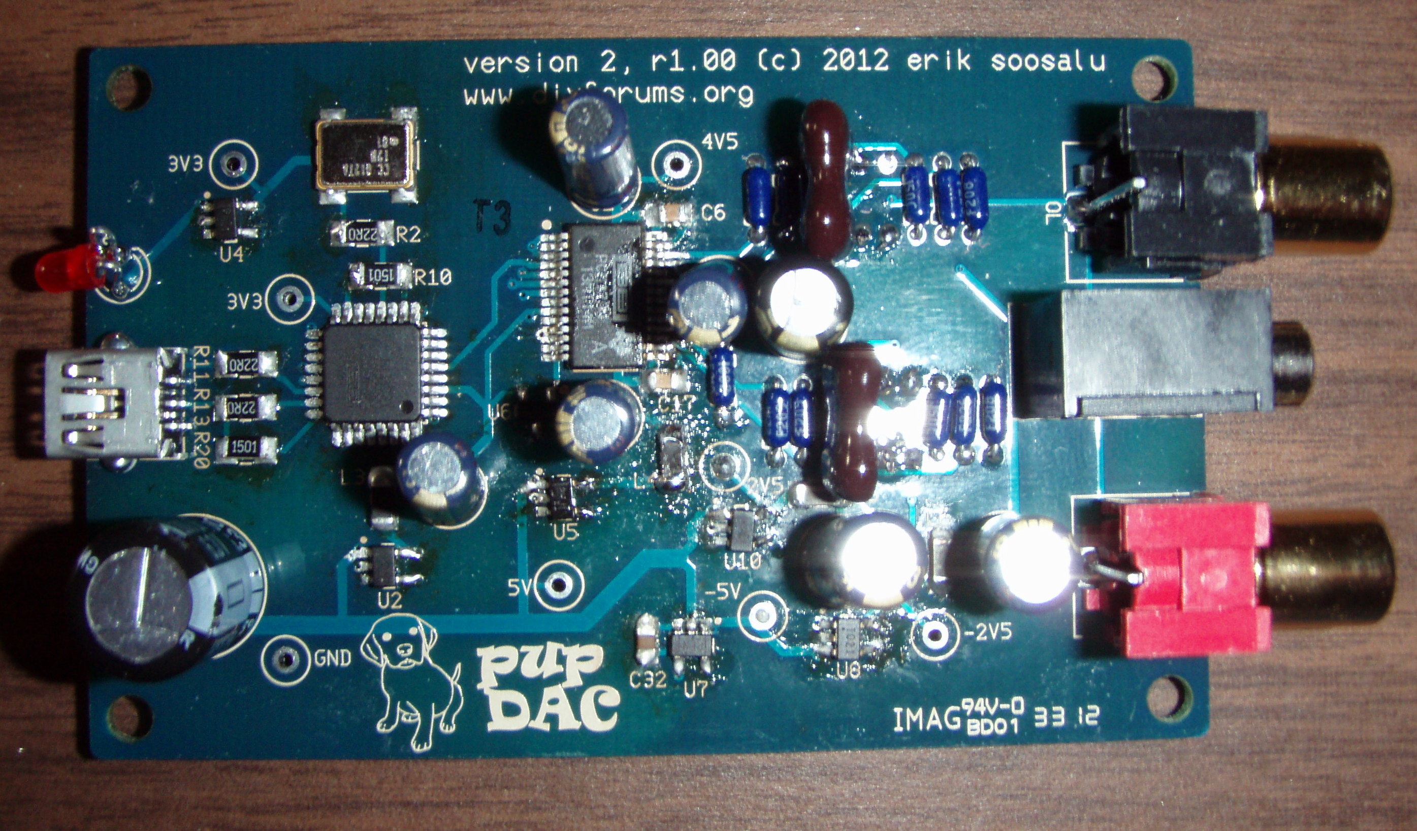
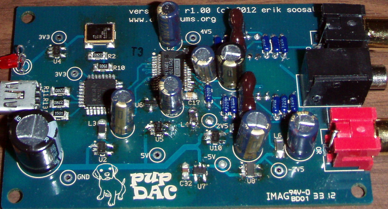
The pupDAC is the newest DAC design from cobaltmute, the designer of the grubDAC and SkeletonDAC.  The pupDAC is a design primarily intended for the finest possible sound from a USB-only-powered DAC.  While DIY-friendly with a now forgiving layout, it is very compact and designed for the tiny Hammond 1455C801 metal case.  We think you'll find the sound from the pupDAC worth the work.
 
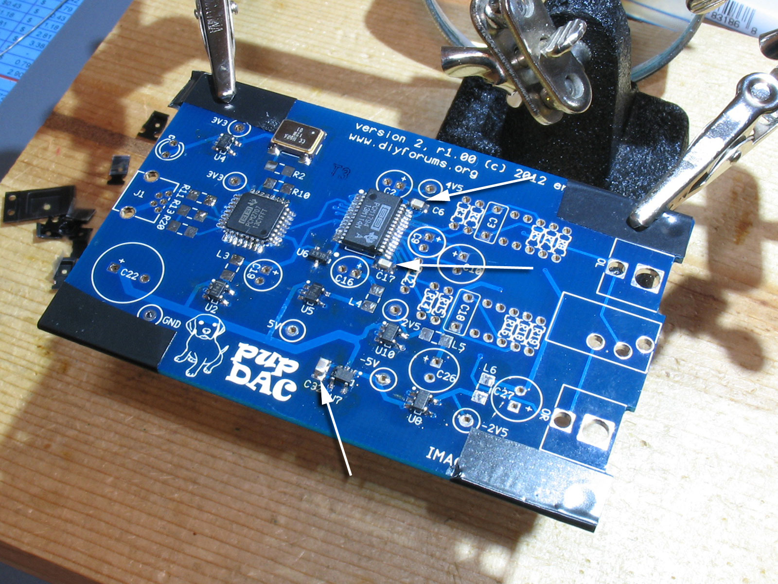
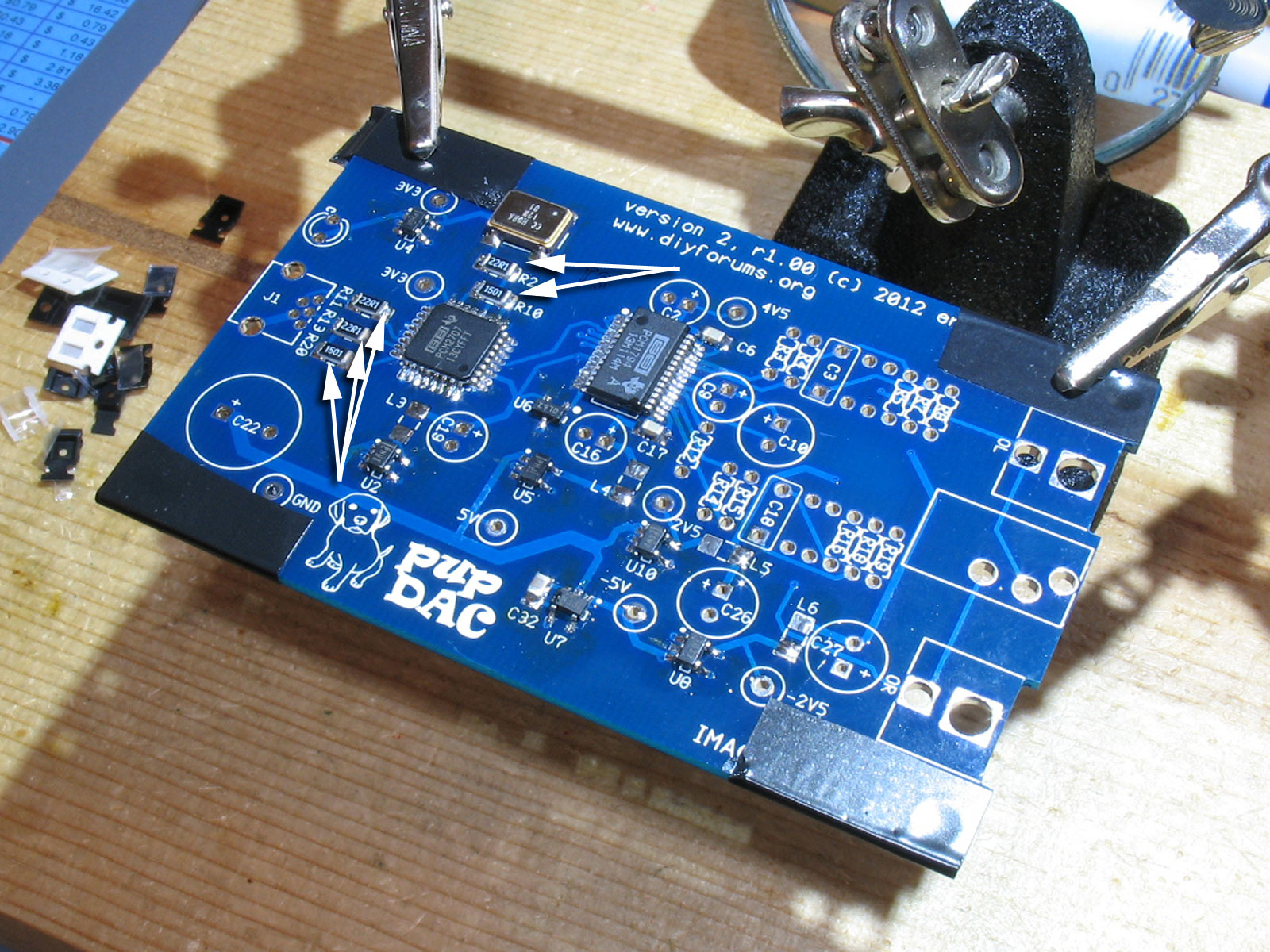
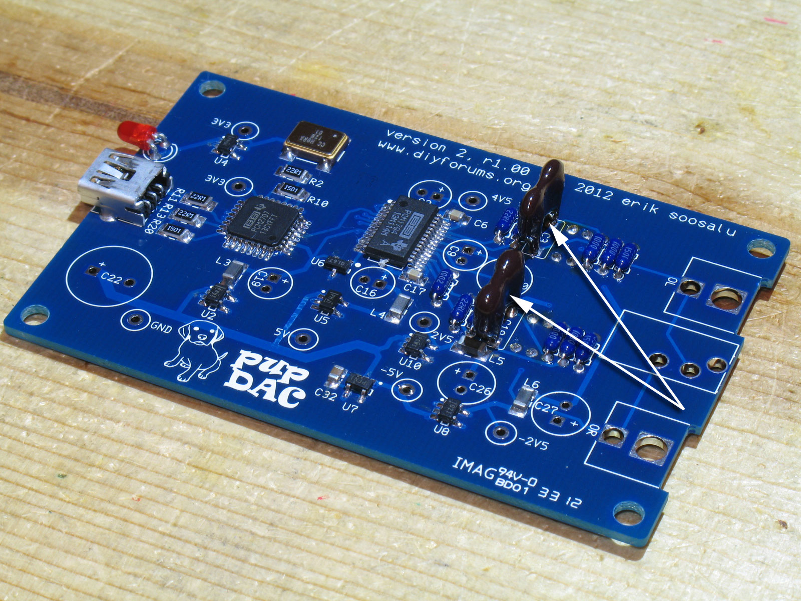
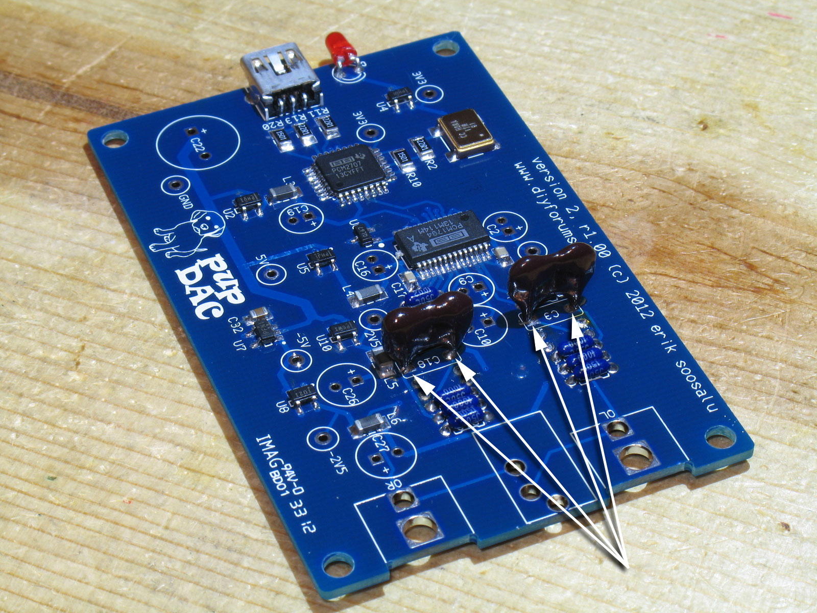
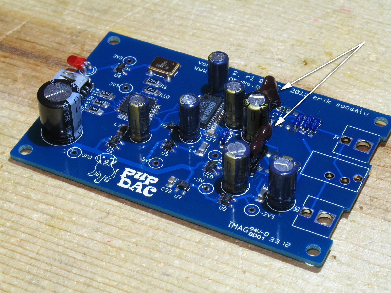
Parts types are no different than what you have found on the AlienDAC, BantamDAC, grubDAC, and SkeletonDAC - TQFP-32, SSOP-28, SOIC-8, SOT-23-5, 1206 and 805 series parts.  It's just that there's so many of them.
wink.gif
  Still, go slow and keep track of the parts and you should have no problem.  The techniques are no different than on any of the DACs mentioned, with a small exception.
 
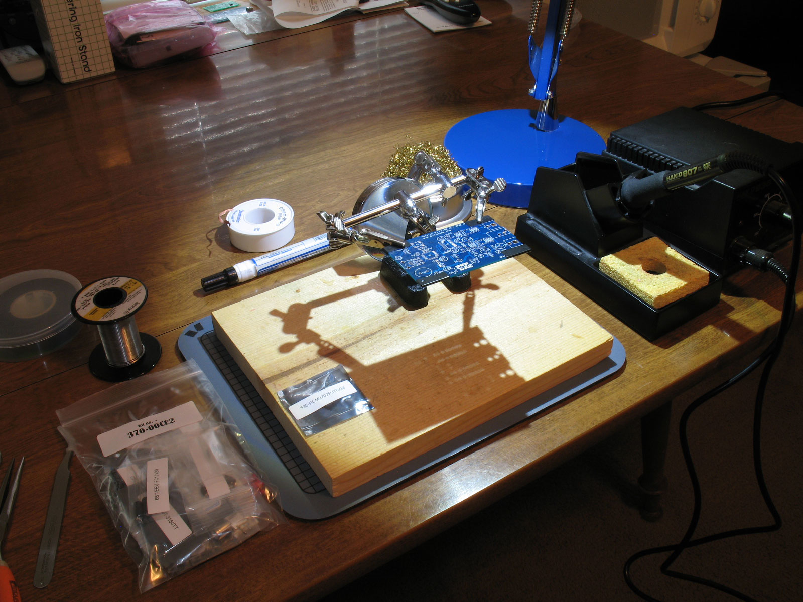
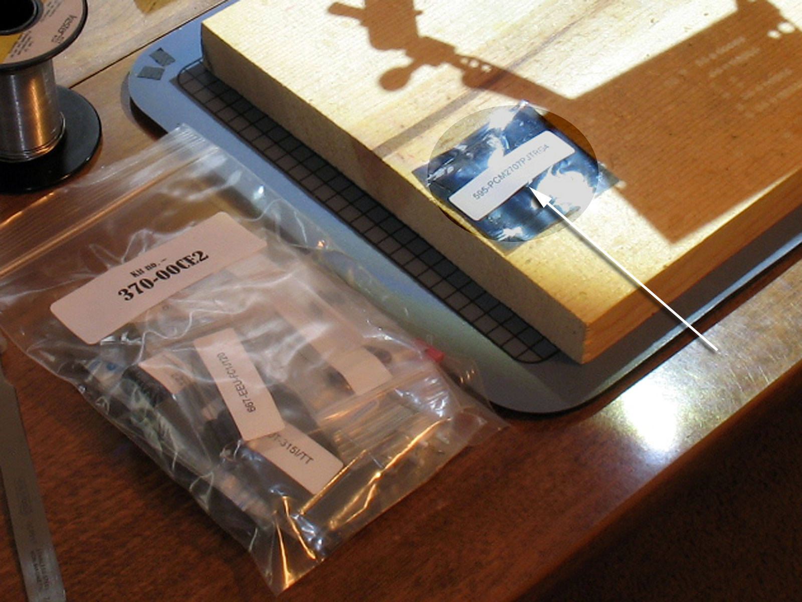
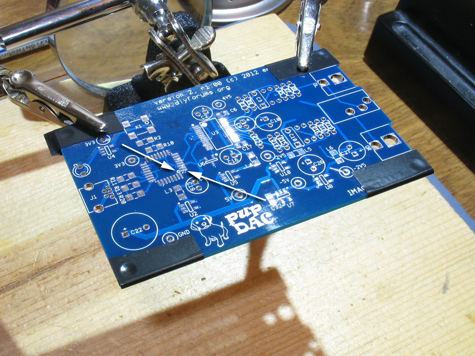
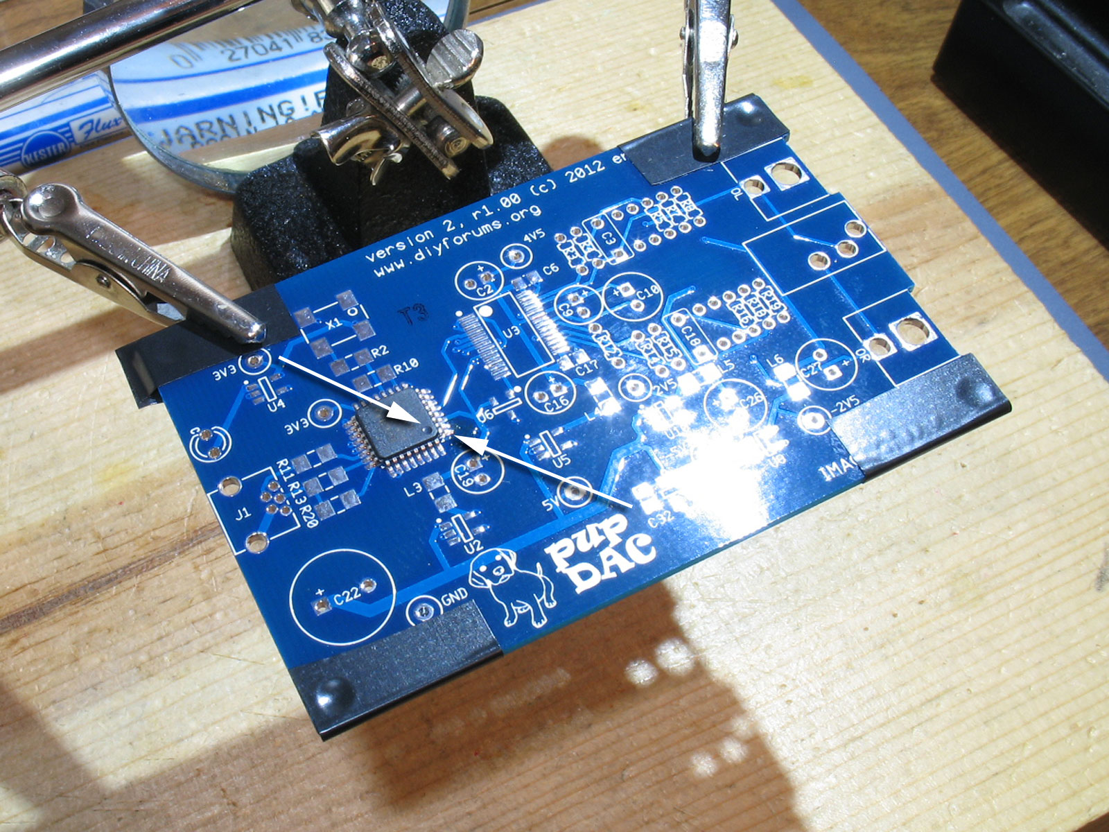
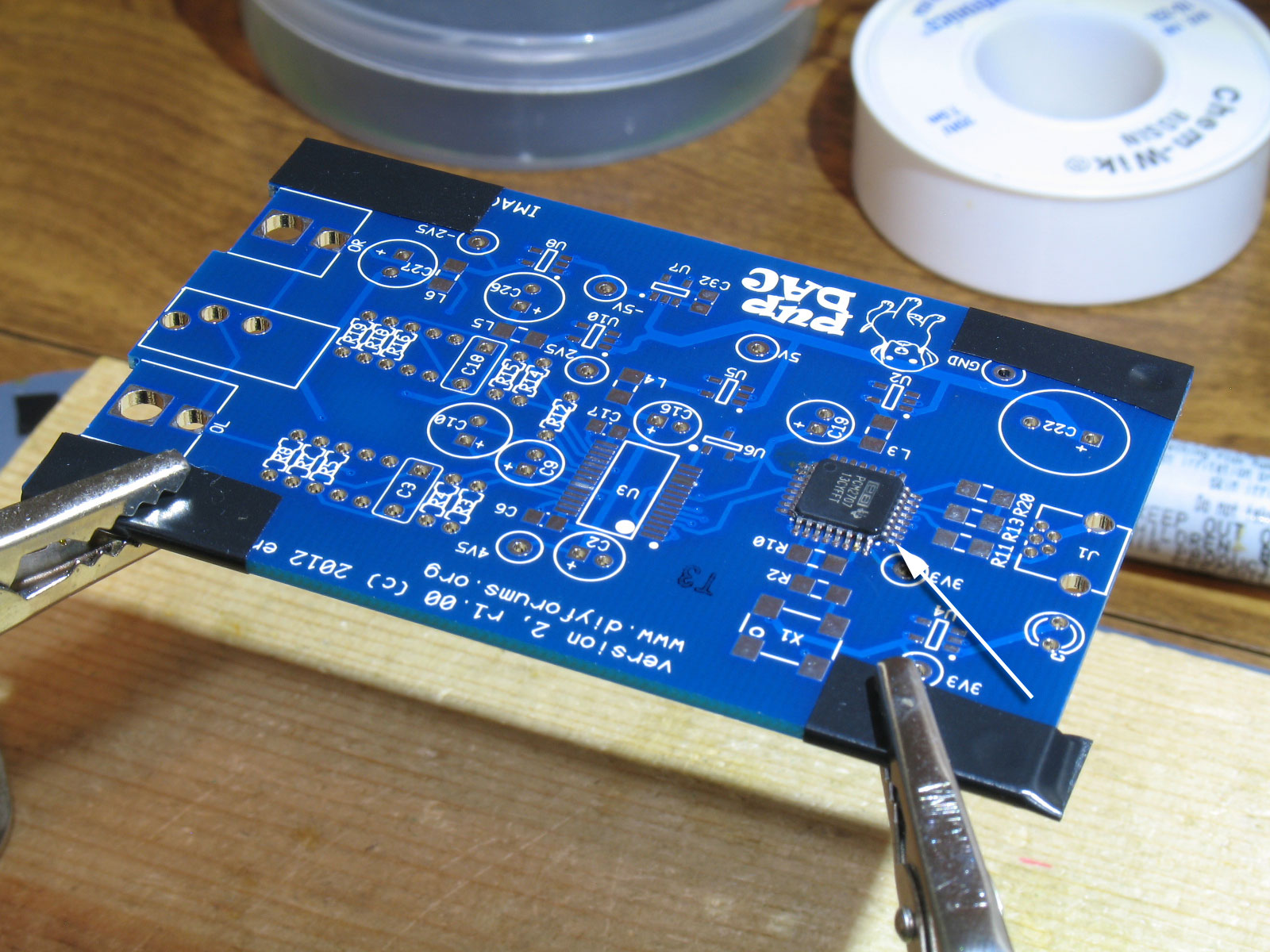
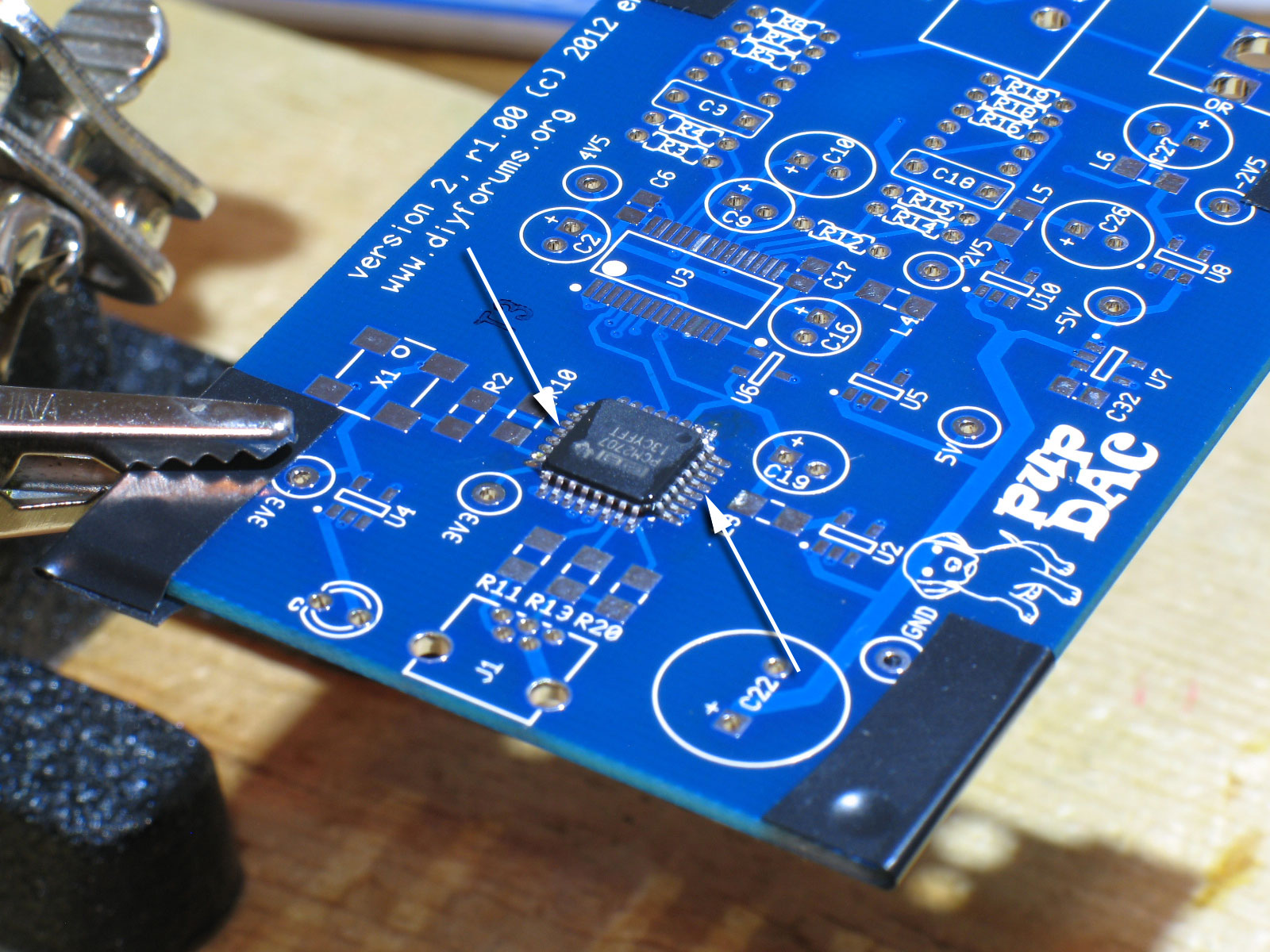
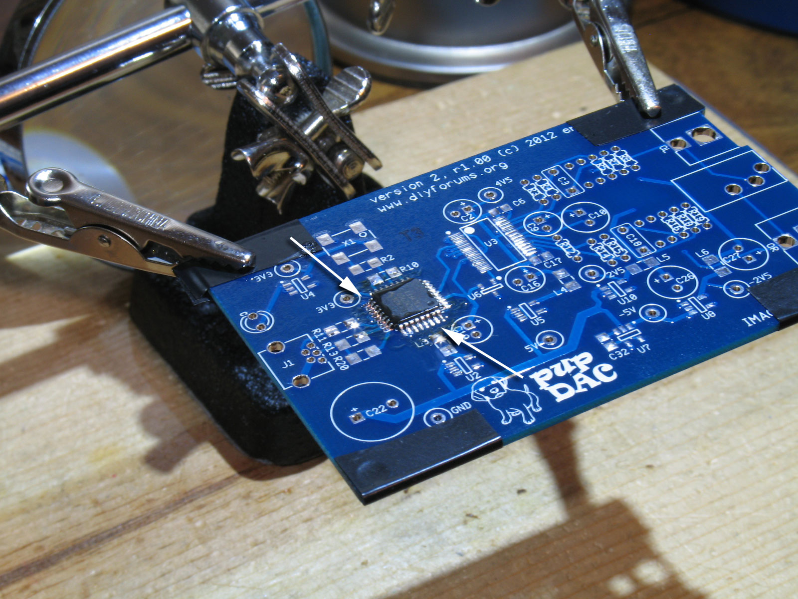
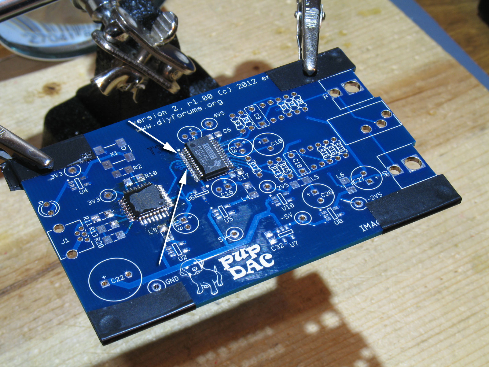
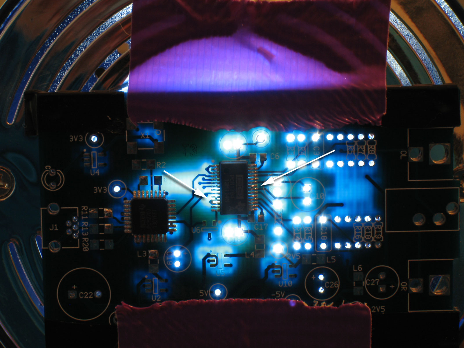
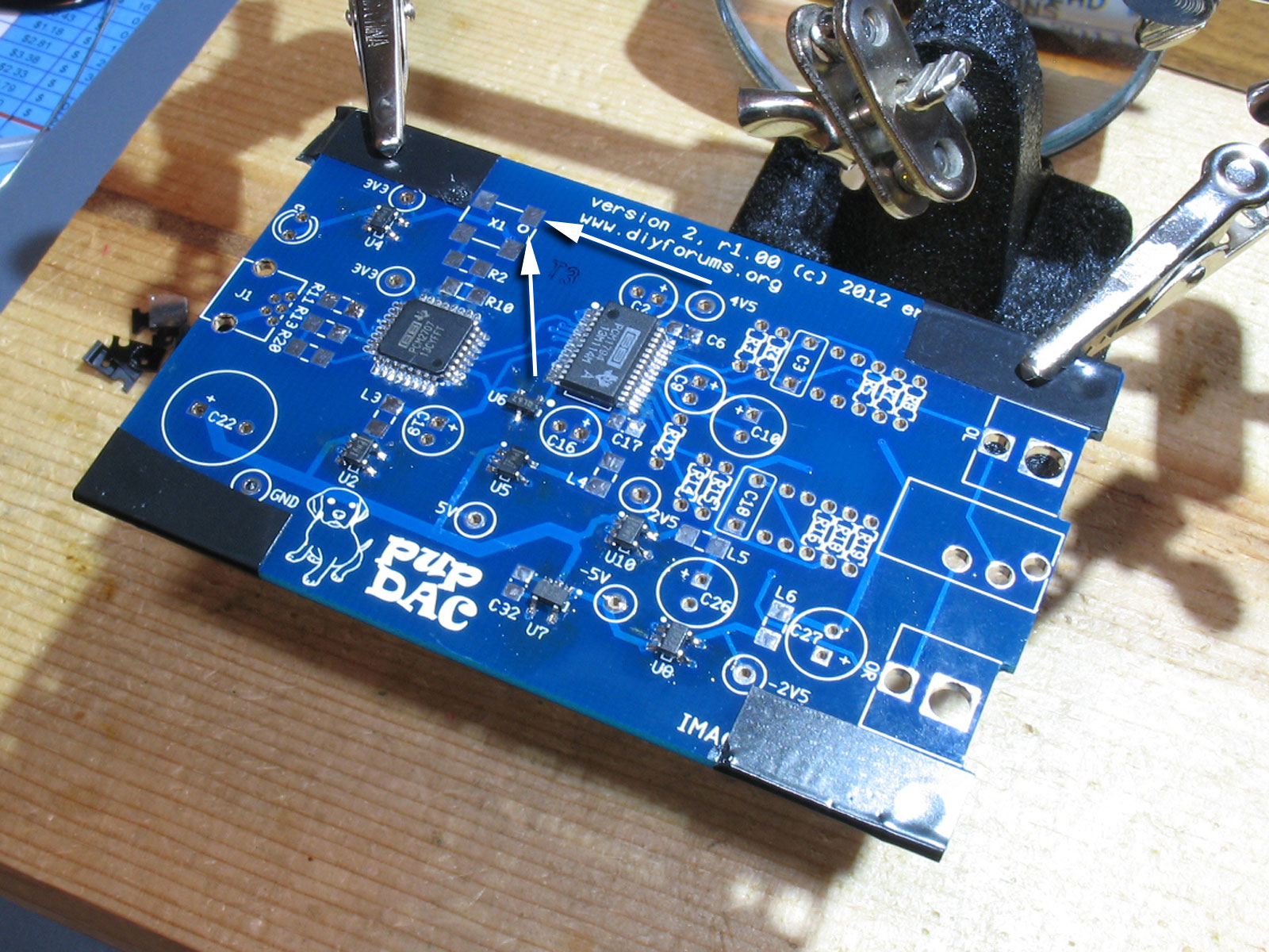
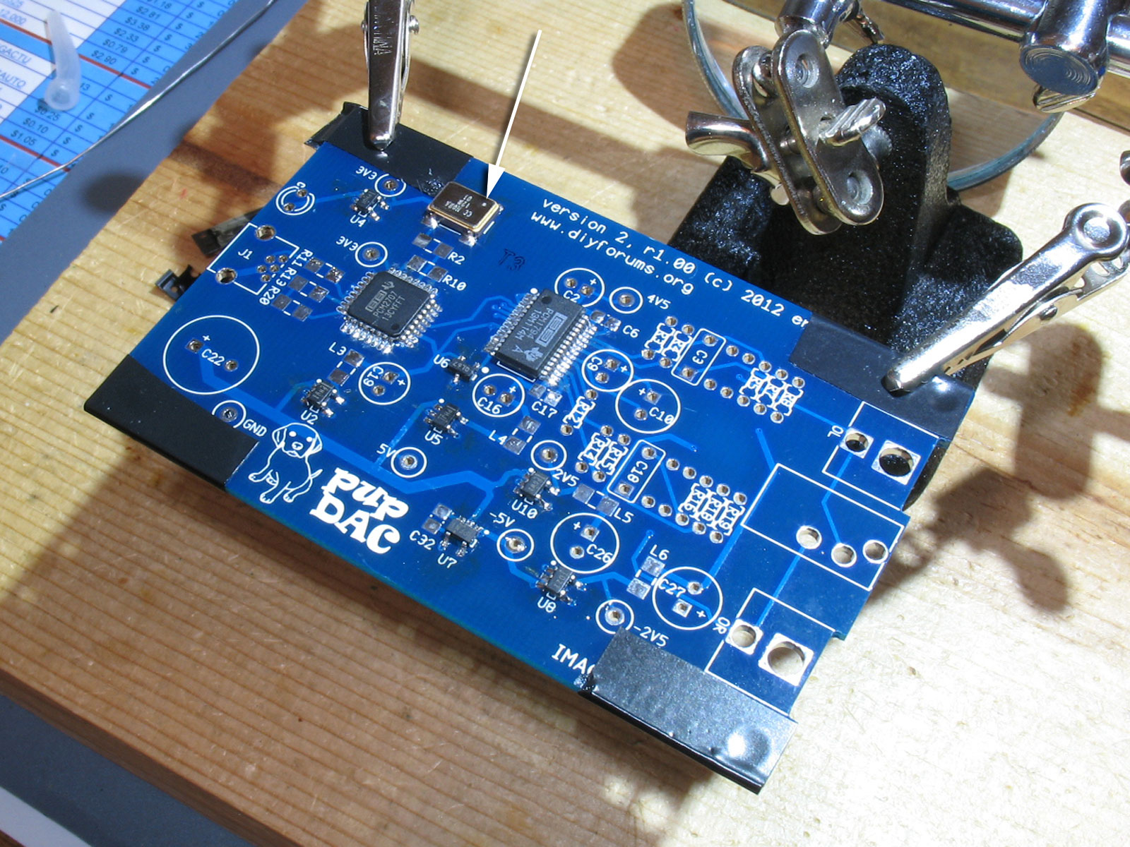
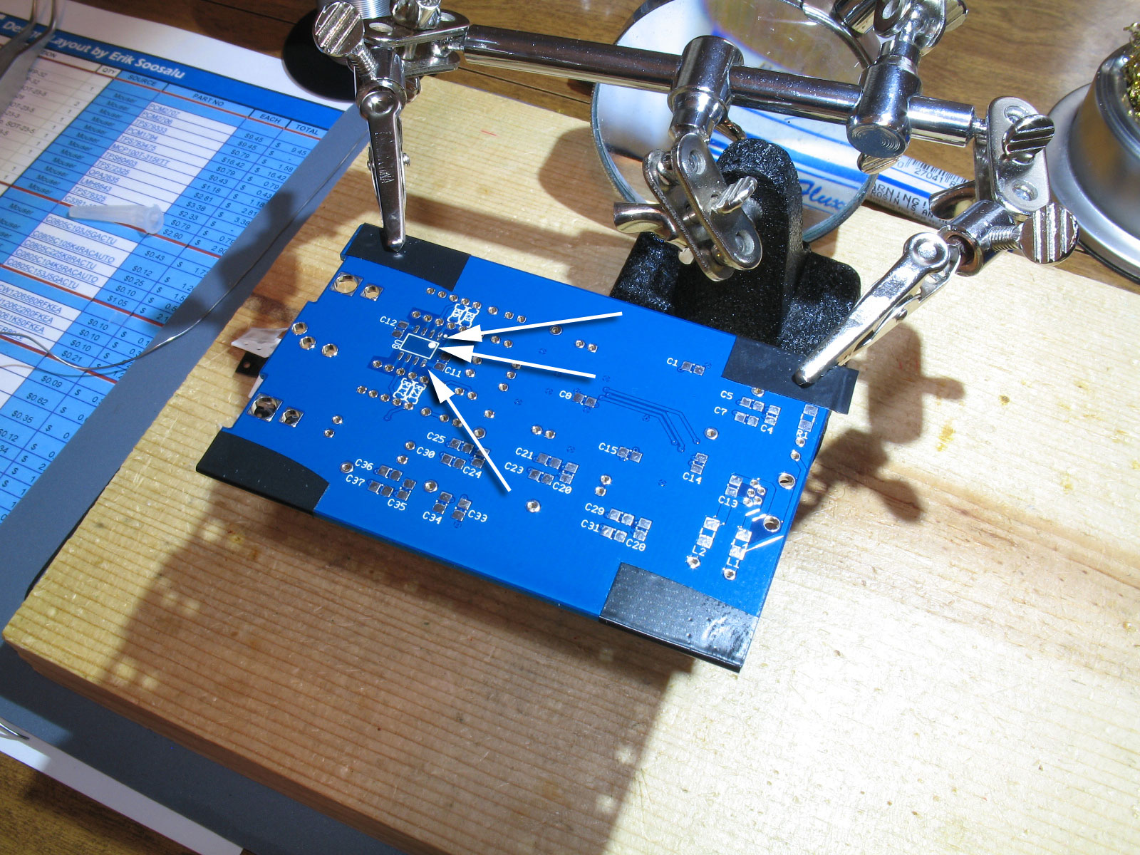
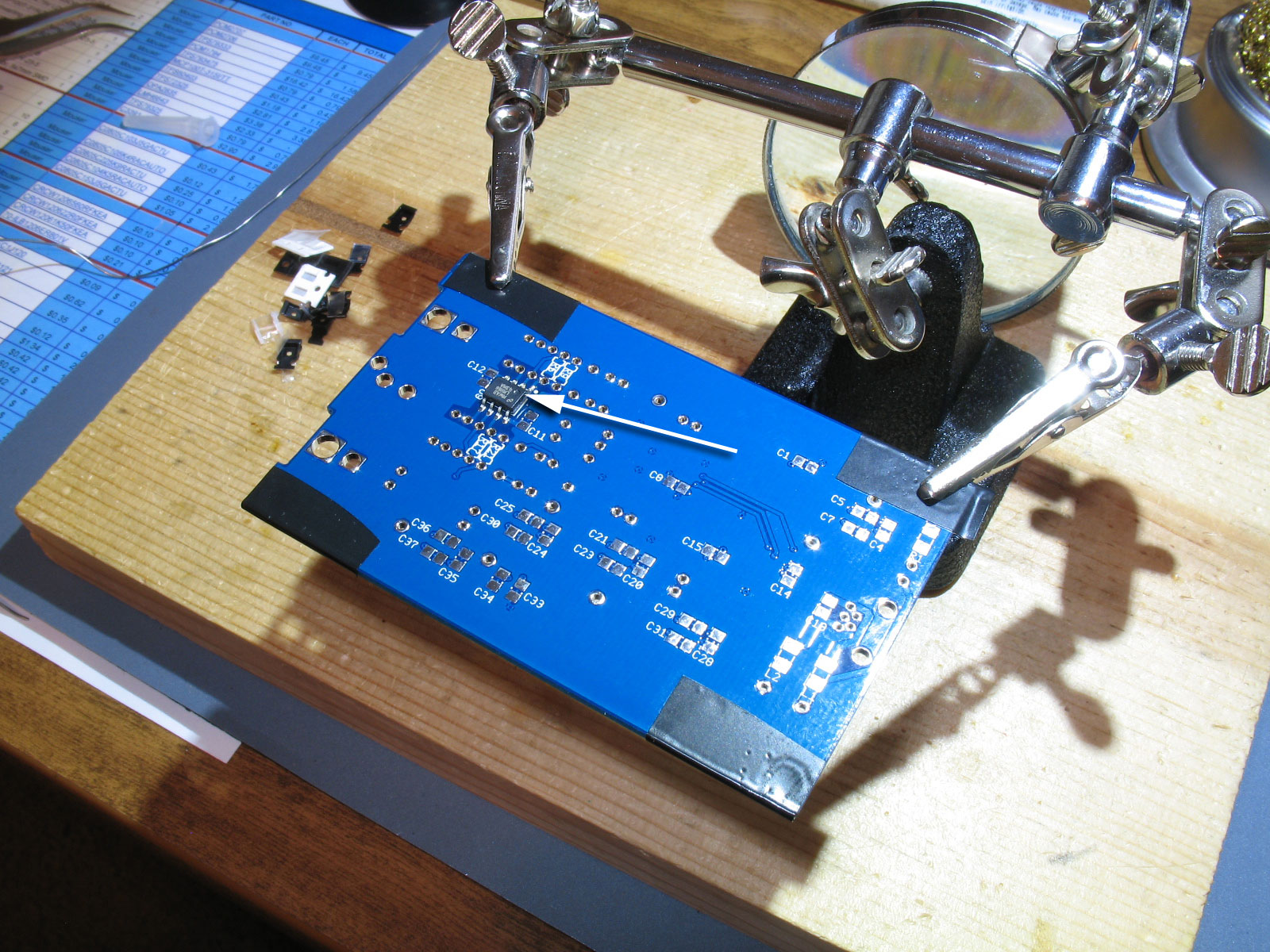
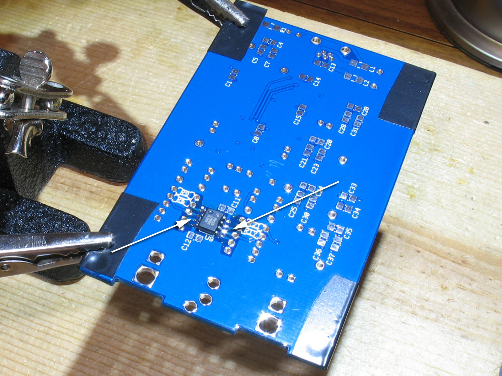
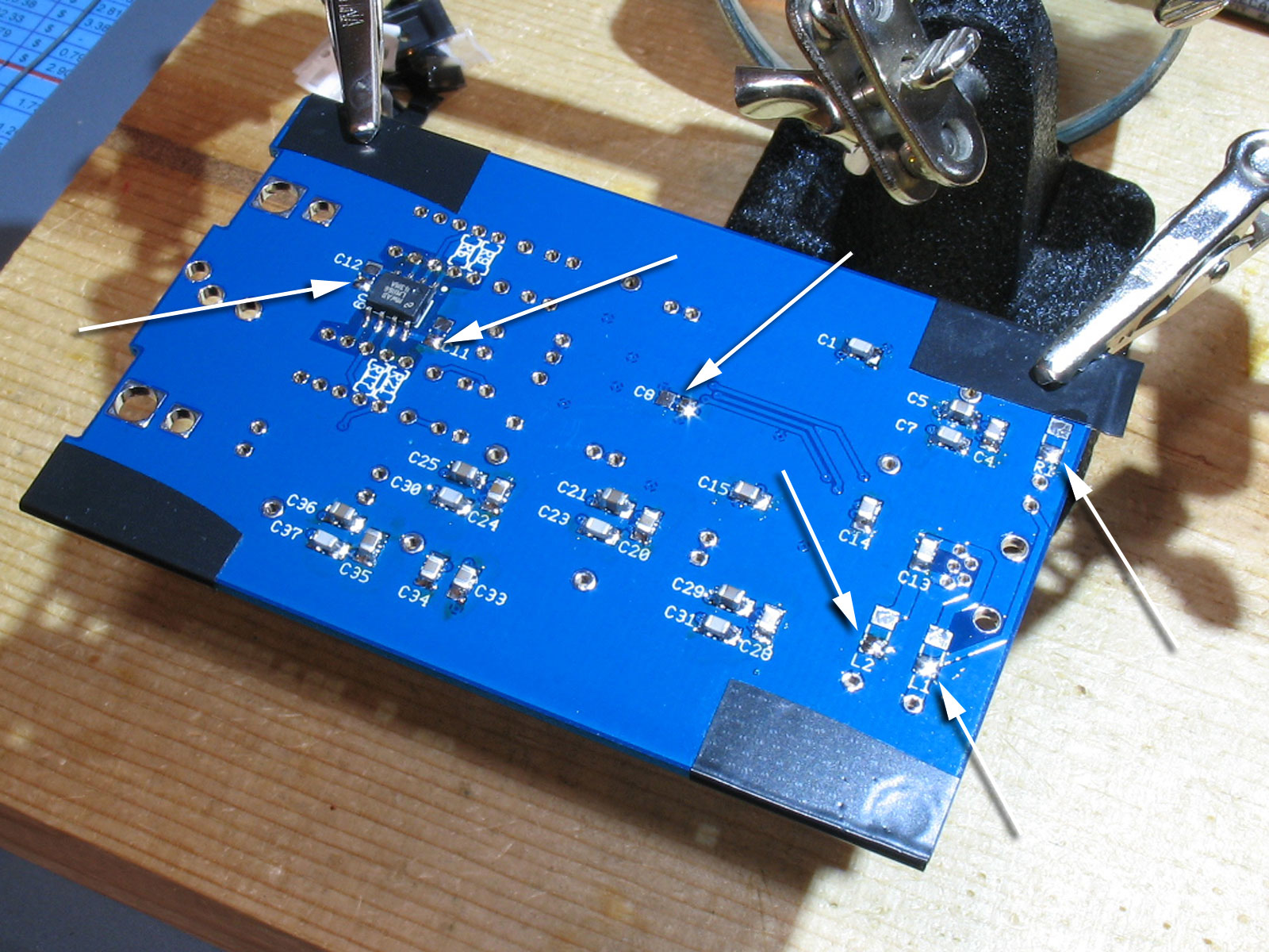
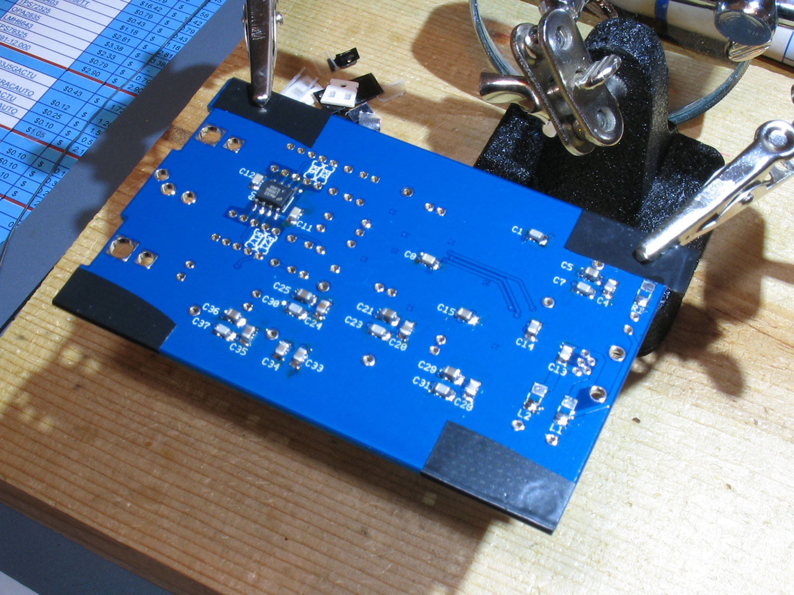
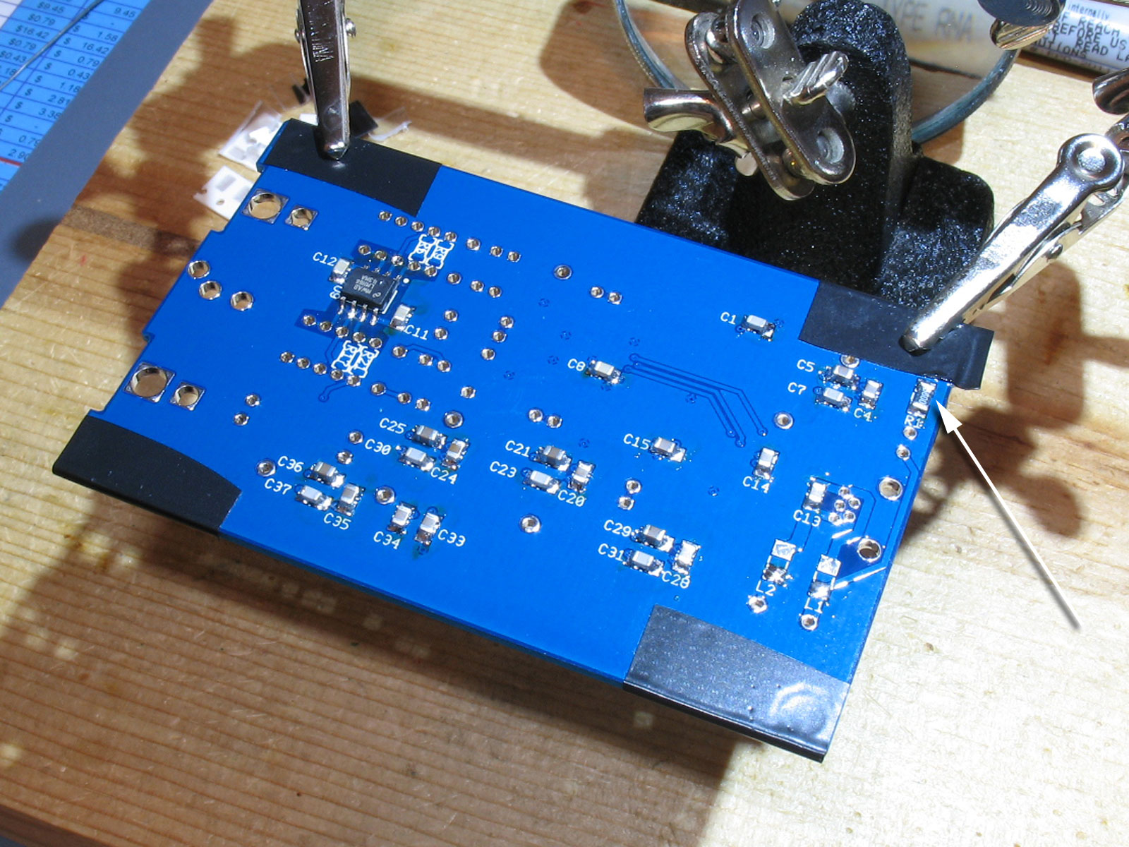
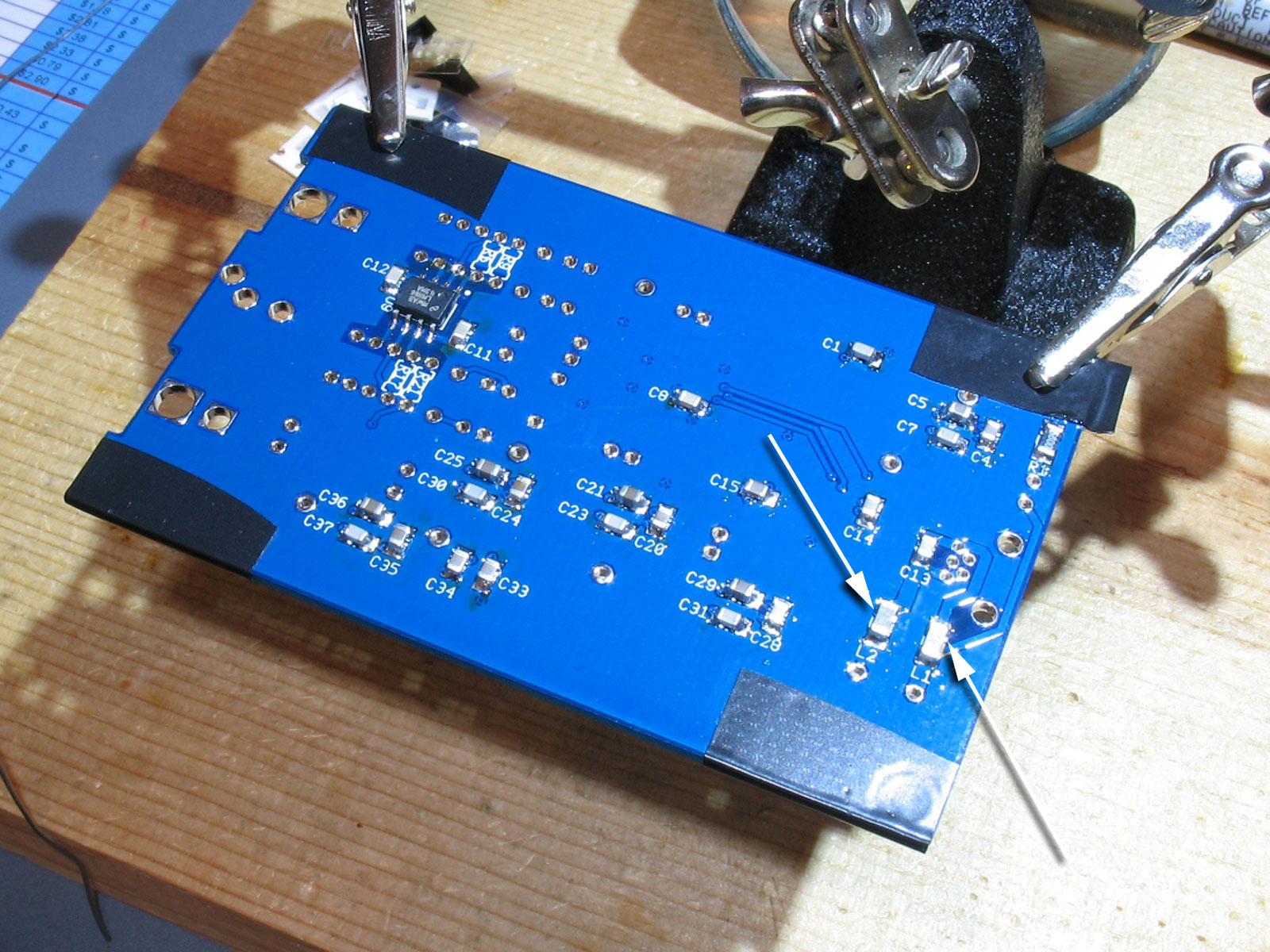
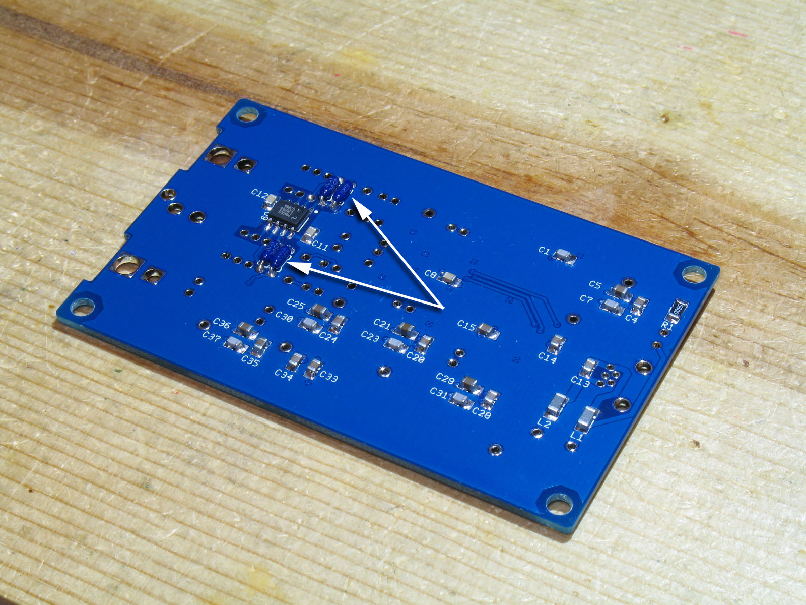
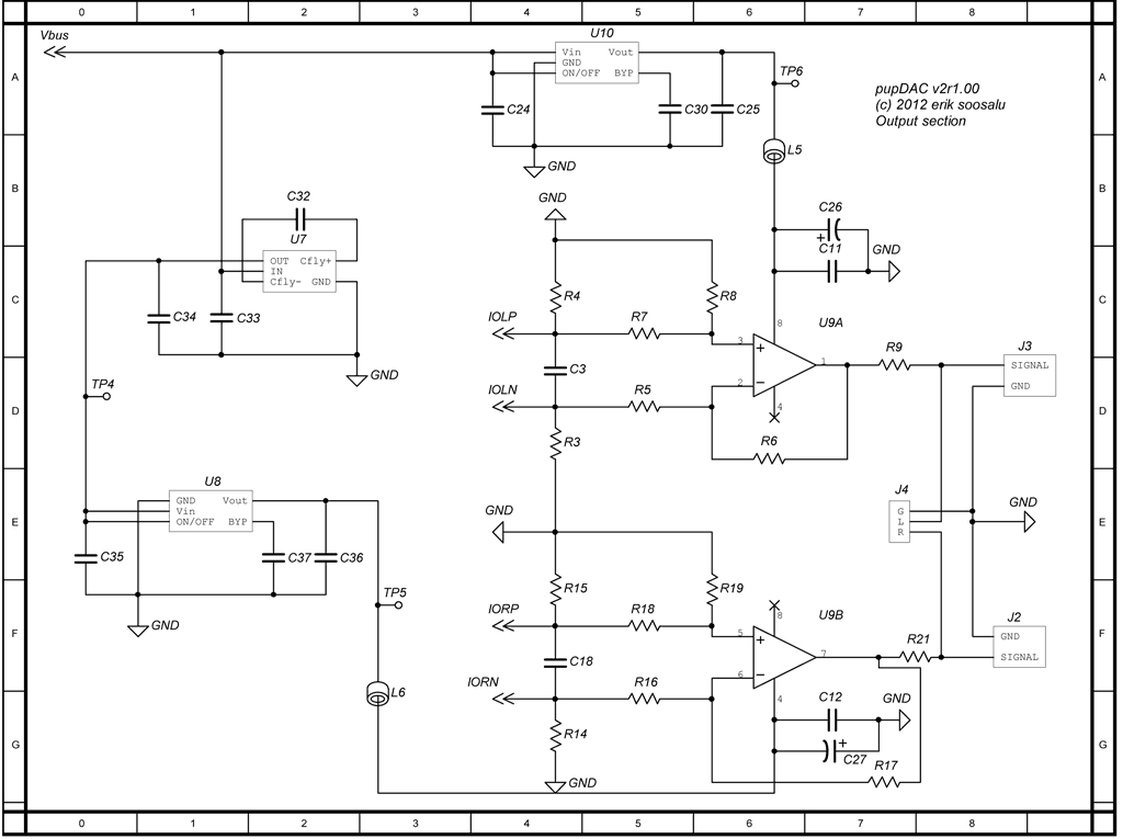
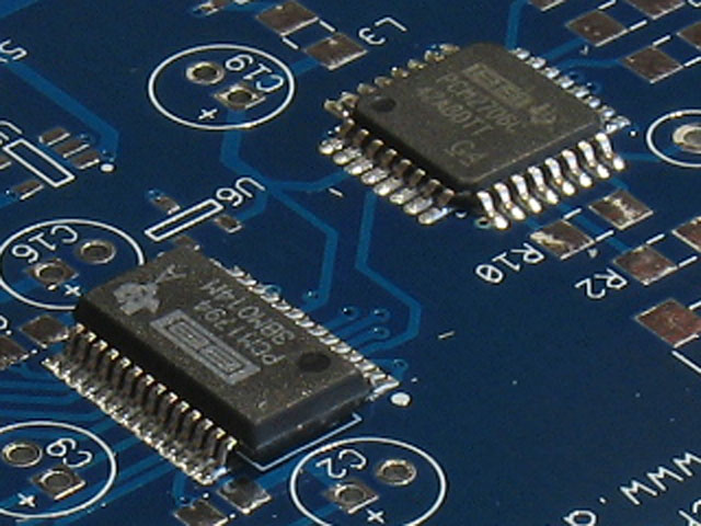
Because there are so many parts on the pupDAC, trouble-shooting the PCM chips later on can be a real issue as access quickly becomes limited as the rest of the parts are installed.  Plus, if you botch those two PCM chips and are unable to fix them, then you've potentially ruined a significant investment in all the other parts you've installed afterwards.  IMHO, the most important thing you can do to ensure a successful build with the pupDAC is stopping, cleaning, inspecting, and testing the installation of the two PCM chips - U1 (PCM2706/7) and U3 (PCM1794).  Get these two chips right before moving on to soldering the rest of the parts and your build should be successful.
 
To many of you, SMD soldering is something new and perhaps a little bit scary.
However, with the right preparation and strategy, you may find it easier in some
respects than through-hole soldering. Like any Do-It-Yourself exercise, success
depends a great deal on proper preparation and tools. SMD has some special traits that make a few tools (one in particular) absolutely necessary.
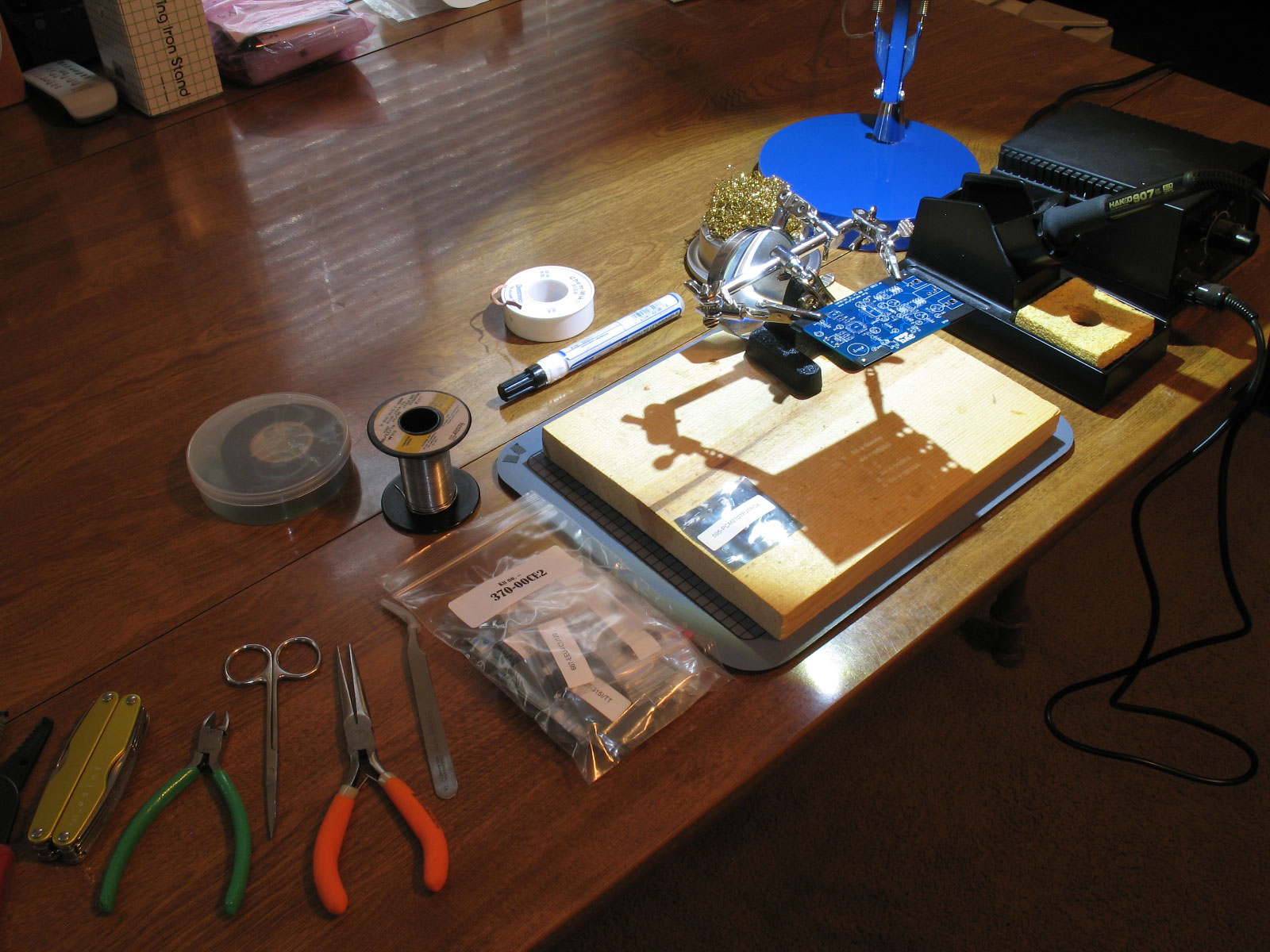
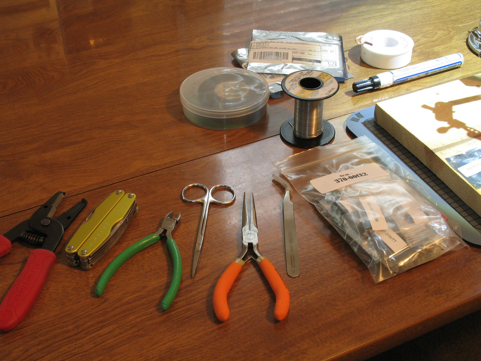
Here's a list of things you need, with the first one an absolute necessity:
  1. tweezers
  2. flux pen
  3. helping hands
  4. small-diameter eutectic solder
  5. small-tip soldering iron
 
Tweezers cannot be over-emphasized. Without a good pair, I have trouble imagining how manual SMD-soldering can even be accomplished. Get a good pair! I use a pair of ESD-safe, bent tip tweezers that I bought at Fry's, but all the good DIY-suppliers have them in stock - Mouser, DigiKey, Allied, Newark, etc. Here's a pic that's similar to the pair that I use (I bought mine at Frys):

Another device that you may find useful is the flux pen. The flux goes down as a
thin liquid and gets sticky very quickly - almost sticky enough to hold a part in
place. The pen form lets you apply the flux where you want it, even on a very small
SMD PCB. I like Kester and stick with their products. The one I use is the Kester
#186. It contains regular activating flux that works great (no water-soluable or
no-clean flux for me).
 
This varies with the individual, but I use a Hakko 936 soldering station, set
at 375 deg.C.  Yes, I've turned up the heat with the pupDAC. It has a rather large ground plane to the grubDAC or SkeletonDAC. I also use a 0.8D chisel tip for the Hakko: 900M-T-0.8D. This is a half-size chisel tip of the standard tip that comes with the Hakko 936 (900M-T-1.6D).  Keep in mind that the temperature setting and my tip selection go hand-in-hand.  If you use a larger tip at that same temperature, it could be that it transmits enough heat to burn.  So be aware of this if you choose to use different stuff - this is only a suggestion/guide and what works for me.
 
Finally, solder is the same solder that I use for all my DIY stuff: Kester 44 eutectic, 63/37, 0.025" diameter.  (As a matter of fact, I bought a 1/2 pound in 2006 and have been using it ever since - on every DIY project, not just DACs.) Larger diameter solder is too big for SMD IMHO, and smaller stuff breaks all the time. Again, I cannot emphasize too much the need for using eutectic solder at 63/37. I have repaired a number of individuals' DIY projects over the years now, and I always shudder when seeing projects that used old 60-40 solder. It makes a real difference in the quality of the joints and there's no excuse - even Radio Shack sells 63/37 eutectic solder.
 
Be sure to review the GrubDAC and SkeletonDAC websites and please check out Tangent's excellent tutorial on SMD soldering: Tangent's Tutorial 3 - SMD Soldering Techniques . I learned how to do SMD soldering with Tangent's methods and with a few exceptions (use of the flux pen), I've been using them ever since.  There are a couple of other excellent tutorials that exist on the web:
The Curious Inventor - Surface Mount Soldering
SMD Soldering Guide by Infidigm
 
Nov 17, 2012 at 9:56 AM Post #2 of 359
Enough of text!!  This is supposed to be photo step-by-step thread, so here goes:

Above you can see my setup before starting to populate the pupDAC PCB.  Again, preparation is all-important.  Make certain that you have plenty of time, you're comfortable, and you're not rushed and nervous.  Good preparation helps to calm the nerves in handling those tiny parts.
wink.gif

 
A closer look to the left at my stuff:

From left to right at bottom: wire strippers (not needed, but just in case), a Leatherman knife (for those odds and ends that come up), quality flush cutters, detail scissors, smooth-jaw pliers ($1.99 Harbor Freight special), curved-tip detail tweezers (see post above), and the pupDAC parts kit as it comes mass-produced and packaged from Mouser.
biggrin.gif

 
A closer look from the right at my stuff:

From left to right at bottom: the pupDAC kit as packaged from Mouser
biggrin.gif
, my building board (1x10 finish-pine) on a non-skid foam mouse pad, the pupDAC PCB held in a set of helping hands ($1.99 Harbor Freight special), on the building board - the Mouser-pupDAC kit package for the PCM2707, and finally - my Hakko 936 (now 6 years old and still going strong).
 
From left to right at top: electrical tape (used to protect the corners of the PCB from the helping hands' alligator clips), my 6-year old 1/2 pound roll of Kester rosin-core eutectic solder (0.025" dia), de-soldering braid with a flux pen, brass wool for soldering iron cleaning (I quit using the water sponge years ago), and a high-intensity lamp.
 
We each have our own working environment.  I'm not saying you have to have all of these things, but they really help me.
 
Nov 17, 2012 at 11:18 AM Post #3 of 359
The first chip that needs to be installed is U1, the PCM2706/7 (both the PCM2706 or PCM2707 will work.  Why this chip first?  Because its pins are on all four sides (TQFP-32).  You need clear access to all four sides to solder it properly.  Once you add a single other part to the PCB, this will become harder.
 
We hope you use the Mouser-produced kit, but keep in mind that the parts are not labeled according to the BOM and the PCB.  They are all individually-labeled, but with the Mouser's part number, not the pupDAC's:

Above is shown the bag for U1 - Mouser has labeled it as their part#, which is a combination of the actual manufacturer's part# along with a Mouser prefix.  For the PCM chips, this is easy.  It's not so easy later on, so be sure to have the pupDAC BOM printed out and handy, so that you can check and verify each part before installing it on the PCB.
 
Here we see the pupDAC PCB again (smudges notwithstanding).  It's held in the helping hands with alligator clips and electrical tape on all four corners for protection.  Note the "T3" stamp.  The pupDAC PCB's have been electrically tested at the manufacturer (Imagineering).  No shorted trace defects to confound your build trouble-shooting.
wink.gif


The first thing we need to do is prepare an anchor point for U1:

Note the arrows.  One is pointing to the alignment dot on the PCB.  Make certain the alignment dot on the PCM chip is in the same position!  The other arrow is pointing to the bottom pad on the right side.  I've applied a bit of solder to this pad.  I'm right-handed, so what I'll do is hold the soldering iron to this pad with my right hand, while my left hand is holding the PCM chip with tweezers.  While the solder on the pad is melted, I'll move the PCM chip into place so that the bottom right pin is positioned into the melted solder.  While still holding the iron and the chip, I'll make certain that the pins line up with all four rows of pads on the PCB.  I'll also make sure that the extended pads leave a bit of room on the outside of all of the pins (the PCM chip will be centered).
 
If you get tired doing this, that's OK.  Remove the tweezers and the soldering iron.  Take a deep breath and relax.  Try again by getting a grip on the chip with the tweezers and then applying the soldering iron to melt the pad again.  Try to position the chip as good as you can - it will make the soldering much easier later on.  Plus, you only have one bit of solder and pad to worry about in this step, so you can keep re-trying as much as you want.  Even then, if the chip is a little rotated, you can actually twist it slightly on the PCB when the solder is cooled.  Just work with it as long as you need to get it in the right position.
 
Here we see U1 in place.  One arrow is pointing to the soldered pad (the only one right now).  The other is pointing to the alignment dot on U1.  It's in the same position as in the pic above on the PCB silkscreen.

 
If you're happy with the positioning of U1, then what we need to do next is to solder an opposite pad, locking U1 into place: 

 
Now that we have two pins soldered, locking U1 into place, we'll proceed with soldering all the rest of the pins:

Here I've fturned the helping hands and PCB at ninety degrees to the building board.  I'll solder the two rows indicated by the arrows.  The two anchor pins we soldered in the previous steps are in the other rows, so we won't be lifting the chip after all of our trouble getting it perfectly aligned.  You can also see that I've applied the flux pen to make the soldering go easier.
 
Bottom line, with the tools I've outlined above, you can actually solder each pin of U1 individually if you'd like.  There's enough space to do this if your solder is on the order of 0.025" dia. and you use the small chisel point that I specified above.  If not, you can use the drag and wipe method (my preference) or the method that you prefer.  I like the drag and wipe because with the extended pads, you can literally solder every pin on the edge, removing the chances of bridges except at the very tip of the pins, where they're easy to access.
 
Here I've turned the PCB around again, applied flux to the other two rows, and soldered them in place.

We're now done with soldering U1!
 
Nov 17, 2012 at 11:30 AM Post #4 of 359
Take a break and use the time to fully inspect your handiwork.  We're going to all of this trouble, remember, because if you get U1 and U3 (the two PCM chips) messed up, your experience with building the pupDAC will not be a fun one.
 
I'm holding the PCB up to a very bright light to check for soldering bridges:

 
My hand got tired, so I decided to tape it up there.  That way, I could check for bridges at my leisure.  A good way to do this is to reference the PCB photos on the pupDAC website.  Note that the arrow is pointing to a "bridge" that's actually a connection of the traces on the PCB.  It is not a soldering bridge.

 
BTW, this lamp is LED-based, so it's bright but not very hot.  You may not want to tape up the PCB like this if you're using an incandescent lamp - damage may result!
 
Anyway, I couldn't find any bridges at this point, so I proceeded on with the rest.
 
Nov 17, 2012 at 12:08 PM Post #6 of 359
Next up is U3, the DAC chip itself (PCM1794).  This chip is SSOP-28 and relatively expensive (almost half the price of an entire grubDAC kit!).  Nevertheless, it is exactly the same chip form as the PCM2702 that was used in the Alien and BantamDACs, and the PCM2704/5 chip used in the SkeletonDAC.  So all techniques and methods you may have used for those chips apply exactly!!
 
Just as with U1, the first thing we want to do is apply solder to a corner pad and use that to position and anchor U3 into place on the PCB.

The bottom arrow is pointing to the bottom right pad where I've applied solder.  This will be the first anchor point.  At top left, the two arrows point out the alignment dots for U3.  Make certain that U3's alignment dot matches these when you position the DAC chip.
 
As with U1 above, grab the U3 chip with your tweezers.  When you got a good grip on it with your left hand, grab the soldering iron with your right and hold it to the bottom right pad on the PCB.  While the solder on the pad is melted and holding the soldering iron in place to keep it melted, move the U3 chip into position so that its bottom right pin is applied to the pad with the melted solder.  Try to align the chip so that the pins match up exactly with both rows of pads.  Try to also position the chip so that there's a bit of clearance on both sides and portions of pads to the outside of the pins on both sides.  As with U1 above, you only have a single pad with solder on it to worry about.  So take your time, get the chip anchored so that it's aligned.  As with U1, even after the solder has cooled on the anchor pad, you may be able to twist the chip slightly on the PCB to give a final alignment.  Use a combination of both so that you have it aligned as good as you can get it.
 
I didn't show it, but I flipped the PCB around to get better access to the top left pad as the second anchor point.

While I had the PCB flipped around, I also proceeded to apply the flux pen to both rows of pins/pads and then soldered the left side.  Which side you get to first doesn't matter as long as you have those opposite anchor pins soldered.
 
Again, I use the drag and wipe method, but I throw some of the other soldering rules out the window.
wink.gif
  The pins are too small and too close together to solder individually, but maybe some of you will be capable of doing that.  For me, after doing a number of these through the years, I CHEAT.  Aligning the soldering iron parallel to the row of pins I'm going to solder, I apply a small (very small) bit of solder to the tip of the iron.  Then I apply it to the pins - on the outside tips and pads.  I may solder two or three pins at a time this way, finishing up with a drag and wipe to clean the excess solder that may result ("rinsing the iron in the brass wool each time before a drag and wipe).  So in effect, I'm applying solder to the outside of the pins, starting at top, and moving down 2 or 3 pins at a time.  Trying to heat the pads/pins with the soldering iron and then to apply the solder to the heated pins, just doesn't work for me.  Instead, apply solder directly to the iron, and then carefully to the pins (on the outside tips), while moving the iron down to the next set of pins at the same time.  I guess that's redundant, but I hope I'm getting the idea across.
 
Once you've made it to the bottom of a row, then finish it off with another couple of drag and wipes.  If you see some pins that look "dry," apply a tiny bit of more solder to the tip of the iron and try again.  Finish up with another drag and wipe.  If you use the brass wool each time before you drag and wipe, the iron will be clean and will actually pick up some extra solder that could form bridges.  So not only does it give a better appearance to the soldered pins, it also serves to clean up excess solder.
 
Here we see both rows of pins soldered:

 
Nov 17, 2012 at 12:09 PM Post #7 of 359
Quote:
If you want to get really good closeups of your board, don't forget my trick with the scanner...


Yep! Great idea!
 
Unfortunately, I need to buy a new scanner.  Seems they never update the drivers on those things and so I have to go back to an old laptop to use mine.
wink.gif

 
Nov 17, 2012 at 12:24 PM Post #8 of 359
Take another break to inspect your handiwork.  Make certain that these chips are soldered correctly before proceeding with the rest.  So, if you don't have access to the scanner, use the light trick again:

Note the arrows.  There are PCB-trace bridges in both places, so don't confuse these with solder bridges that you may have created.
 
Another method of checking for bridges is to use your DMM.  Place a probe on one of the pins as it exits the chip (not on the solder or pad).  Follow the trace connected to that pin to some other place on the PCB.  Place the other probe, there.  If you read -0- resistance, then you have a good connection.  Similarly, follow the trace from an adjacent pin and place the other probe, there while still using the first probe at the pin's exist from the chip.  If you read something other than -0- resistance, then you should not have a cross connection/bridge.  Refer to the schematic for the pins that are grounded and simply place a probe at GND.  Also refer to the schematic for pins that may be connected to each other purposefully as with the arrows above.
 
You can also use this time to re-check the U1 chip.
 
When you are satisfied that you've got these chips soldered OK, then proceed on with the rest of the build.
 
Nov 17, 2012 at 1:34 PM Post #9 of 359
At this point, you have a lot of tiny SMD parts left to solder.  As mentioned previously, the Beezar/Mouser kit has been packaged from Mouser with their part numbers on the bags.  So, you need the BOM to reference the part numbers with the pupDAC part #'s used on the PCB:

 
Next up are the rest of the "U" chips.  All the remaining "U" chips on the top side of the PCB are TPS regulator chips, except for two.  One is a supervisory controller, U6, and the other one is the charge pump, U7.  Except for the supervisory controller which is SOT-23-3, all the other "U" parts are SOT-23-5. The five-pin chips have 3 pins on one side and 2 pins on the other.  I've found it's easiest to anchor and place the chip using the middle pin on the 3-pin side.
 
Note that the single remaining "U" chip is the U9 opamp that gets soldered on the back side.
 

Here the arrows are pointing out the solder that I've placed on the middle pins of all the remaining "U" parts, except for one outside pin on U6.  These pads will be used to place the U chips on the PCB.  The method is the same as that of the PCM chips: while grasping the part with tweezers using your left hand, use your right hand to melt the solder on the pad with the soldering iron.  Holding the soldering iron in place to keep the solder melted, move the part's pin in position onto the pad with the melted solder.  Check the alignment, then remove the soldering iron and let cool.  Then remove the tweezers.
 
Using the middle pin on the 3-pin rows like this gives you maximum accessibility to solder all of the other pins.
 
Since almost all of the 3-pin rows are on the left side, I've flipped the PCB and helping hands around so that I can access the soldered pad with the soldering iron in my right hand.  Working from right to left across the PCB, the first chip has been placed and soldered into position:

 
The rest of the chips follow.  Move the PCB and helping hands around as needed to access and solder all the remaining pins:

 
Next up is the oscillator, X1.

The arrows point to one pad as the anchor pad (same old method) and the other arrow is pointing at the locating dot.  Be certain you align X1 accordingly.
 
Here we see X1 soldered in place.  Note the locating dot on top of the part.  One important item to remember: the solder should wick up the sides of the oscillator, but do not use so much solder that it bridges over to the metal top.  If so, you will have shorted the oscillator and you'll need to clean it up:

 
Here we have the 805 capacitors, next:

 
The 1206 resistors - try to be organized and have the printing oriented in one direction:

 
Finally, there are three 1206 ferrites on the top side.  Note that all the ferrite "L" chips are the same, so no confusion possible, here: 

 
You've now finished all the SMD parts on the top side of the PCB!
 
Nov 17, 2012 at 2:39 PM Post #10 of 359
Hmm ... I've always wondered when posting one of these, what does it take to start a 2nd page?  This seems awfully long for one page - oh, well.
 
Next up is the backside of the PCB - the opamp, lots of little 805 capacitors, a couple of ferrites, and one 1206 resistor.
 
Here we see the reverse side of the PCB:

The arrows indicate the anchor pad I'm going to use for the opamp.  Also, pay close attention to the locating dots ont he silkscreen.  TI is being a little tricky these days - the OPA2835 comes with a line drawn across the width of the opamp on the locating side.  If you use this opamp, solder with the line on the end where the locating dot is on the PCB.  The LMH opamp has a circular dent in the top of the opamp that forms a permanent "dot."
 

The arrow indicates the circular dent in the LMH opamp.  The anchor pin is soldered and the opamp is aligned.
 
IMHO, an SOIC-8 opamp such as the ones the pupDAC use are just about the easiest SMD part to solder.  There is plenty of clearance between the pins to individually solder each pin. 

I've soldered an opposite anchor pin to the first one and then soldered the rest of the pins, one at a time.  Finish off with a drag and wipe on each side, if desired.
 
I kind of jumped ahead at this point with my photos, but no matter.  This is about 3/4 of the way through with soldering all the 805 capacitors on the reverse side of the PCB.  Same old method is used - I actually prime all the pads (one each) of the rest of the parts, then start with the smallest (805 capacitors).  Melt the pad you've applied solder on, and while holding the soldering iron to keep the solder melted, position the part in place with your tweezers.  When you have the part properly positioned, release the soldering, let the solder cool/harden, and then release the tweezers.  Go back and solder the remaining pad at your convenience.

Note the arrows indicating the remaining pads that I've "primed" all at once, including the single 1206 resistor pad and the two remaining ferrite pads.
 
Here we see all of the capacitors finished:

 
Next up is the resistor:

 
And the remaining two ferrites:

 
Whoa!!  We've finished every SMD part on the board.  Take a short break at this point to inspect all of the SMD parts on the reverse side.  Make certain that you haven't forgotten to solder a remaining pad somewhere.  Also, take this time to fully rinse the PCB as shown in the next post.
 
The easy through-hole stuff is next!
 
Nov 17, 2012 at 2:50 PM Post #11 of 359
I like to clean everything up at this point.  Why?  Because the SMD parts can be immersed completely, whereas through-hole electrolytics are not completely sealed and could be hurt by doing this.  At any rate, it gets things very clean among all those tiny pins.  Wait till later and you may have all sorts of trouble getting things cleaned.
 
I use 91% isopropyl alcohol from Walmart for cleaning all my projects.  It leaves no residue once the board is completely rinsed and it readily dissolves flux.  The use of an old toothbrush can help to get those troublesome flux patches off where the simple soaking does not.


One thing to be aware of - the latest chips from TI use a different case material and is actually hygroscopic.  The pins are sealed at the case body, but the body itself may absorb moisture.  This is nothing to worry about except when you've rinsed at the end and you're ready to plug it in - don't.  Wait for a few hours, use a hair dryer, put the PCB out in the sun, etc. to make certain that things are dry under and inside the chips.  Otherwise, you'll drive yourself crazy trying to figure out why your DAC doesn't work or seems to de-activate itself every few minutes.
wink.gif

 
More later ...
 
Nov 18, 2012 at 12:15 PM Post #14 of 359
Thanks for the compliments, guys!
 
On to the through-hole parts!
 

The small precision resistors are first, since they're the lowest in height except for the SMD parts.  I like to solder in the resistors on the back, first.  Then we're done with everything on the reverse side of the PCB.  Why are there through-hole resistors on the reverse side?  Cobaltmute's design minimizes the offset from the opamp by making the lead-length and traces from these particular resistors as short as possible.
 
As always, ensure that the rating is visible from the top when you install them.  Precision resistors such as these are not color-coded.  Therefore, if you don't ensure that the rating is on top and visible, you'll have a hard time confirming the proper values if you need to troubleshoot.  (DMM resistance measurements are often inconclusive on a populated PCB - the resistors are often in parallel with other resistors or devices, making it difficult to get a one-to-one reading on the resistor's value.)
 
Warning!  Ensure that you pull the leads all the way through and get these resistors as flush as possible.  The pupDAC PCB will be placed in the lowest slot of the Beezar/Hammond custom case.  There is less than 2mm clearance between the bottom surface of the PCB and the inside-bottom of the case!  You will also need to trim all the leads from the bottom of the PCB to guard against shorting.  More about that later when we finish the through-hole parts.
 
Trim the leads and continue on with the resistors on the top side:

Don't forget R12 over there in the middle by itself!
 
Next up is the LED.  Since we're building this for the custom Beezar/Hammond case, we need to know how to install the LED so that it lines up with the machined hole in the endplate.

Bend the leads at right angles as shown - just behind the point where the leads "neck-down" to entire the LED housing.  This is clearer in the next pics, but bottom line, you want to install the LED so that the LED is horizontal and parallel to the PCB, with the flange resting flush and at the edge of the PCB.
 
I guess it's a Canadian thing
wink.gif
wink.gif
, but cobaltmute labels the "Cathode" lead of the LED instead of the long "+" lead.
wink.gif
  That's the "-" lead or the SHORT one.  So be certain: The short lead goes into the "C" hole.
 
Here you can see more clearly exactly where to make the bend.  If for some reason, you end up with an LED that doesn't have leads shaped like this, then just be certain that you bend the leads so that the flange is flush to the PCB and at the edge of the board:

 
Another view to make sure:

Done this way, it lines up perfectly with the machined hole in the endplate.
 
Next up in the lowest-to-tallest part hierarchy is the mini-USB jack:

Remember here, too, that you're installing this to line up with a pre-machined endplate.  Make certain that the mini-USB jack is absolutely flush to the PCB (note that only the front half is actually flush to the PCB - check the drawing of the part if you're uncertain) and square (not turned at an angle).  Also, the mini-USB is a mechanical connection.  It will undergo a lot of stress with plugging and un-plugging a USB cable.  If you use the case bezels, there is no other support except for the solder connections at the PCB.  The arrow is pointing to the snap tabs that provide the greatest structural support to the jack.  Ensure that the pad hole is fully filled with solder from the bottom and that when you make the solder connection, you get good wicking to the top side as is shown here.
 
Another view showing the "structural" solder wicking to the top side:

 
Next are the Mica capacitors, C3 and C18:

These things seem to have the worst quality control when it comes to sizing tolerances of any type of capacitor.  You will find different sizes between almost any two in a bag.  That's OK - just try to make sure that you pull the leads through as far as you can.  (You may see some through-hole plating chips popping out of the pads as if you're re-drilling the holes.)  This minimizes the lead length and ensures that you haven't exceeded your height clearances.  You may still need to bend them like wings to fit in the the electrolytic capacitor, C10, but more on that later.
 
Here's another view illustrating how the caps are pulled through so that no bare leads are showing.  You may even slightly crack some of the epoxy coating on the high-part of the leads, but that's OK as long as you don't damage the capacitor's main body overall.

 
Time to install the electrolytic capacitors!  It's a judgment call as to which is taller - the electrolytic capacitors or the RCA jacks.  The drawings will tell you that the RCA jacks are a tad shorter, but I haven't found that to be the case in real practice.  I think when you get electrolytics of this size, the variance in the rubber plug exposed at the bottom of the cap is fairly high.  Regardless, it's quite easy to hang the PCB over the building board so that you can get the RCA jacks flush to the PCB later on.
 
My method in installing electrolytic capacitors is to place them all in the holes on the PCB.  Take my pine piece building board, turn it over and hold it on top of the capacitors while holding the PCB in my other hand.  Then while holding PCB on bottom and pine board on top with both hands, I turn over the entire assembly so that the pine board is back on the bottom and the bottom of the PCB with the capacitor leads are on top - ready for soldering.
 
While pressing down on the bottom of the PCB to get the upside-down capacitors flush, I solder one lead each on each capacitor.  When that's done for all the capacitors, I flip the PCB over and check the caps for alignment and square them.  Them I flip the PCB back over and solder the remaining leads.
 
C2, C9, C16, C19, C10, C26, and C27 are close enough in height to be soldered at the same time using the procedure described above.  C22 is just enough taller that you should probably solder that one in after all the others.
 
As mentioned before, the Mica caps (as packaged in the Beezar/Mouser kit packaging) are too big to allow enough clearance for C10.  I simply bend the Mica caps like "wings" to either side of C19 as show below: 

 
Another view of the electrolytic capacitors installed and the Mica caps bent to either side of C10:

 
The RCA jacks are straight forward.  Install them before the 3.5mm/1/8" stereo jack.  (The 1/8" stereo mini-jack is the tallest part on the pupDAC.).  Note that the solder joints for these are also structural in nature.  However, they have real, bent-spring snap tabs at the ground connections, so the pad holes are actually too big to fill-in completely with solder.  You will end up melting all the plastic housing if you attempt to do that.  Instead, ensure that there's ample solder around the tab and fill-in completely the signal connection pads (the ones in back), so that they proved some structural support.  Note that the plastic tabs on the bottom in the front fit over the thin cutouts at the edge of the PCB.  This helps to lock them into proper position and ensures that the jacks are flush against the PCB at the top surface and front edge.

Install the remaining 3.5mm/1/8" stereo mini-jack so that it's flush and square with the PCB.  Be careful with these parts.  It may be best to let them cool somewhat inbetween soldering their tabs.  The entire housing for all three jacks is plastic and can be easily melted if exposed to too much heat for too long.
 
FINISHED!!  Another view of our completed pupDAC:

 
Prior to final clean and rinsing, be certain to trim all the leads underneath the PCB.  This includes the leads/tabs for all the output jacks.  As mentioned previously, there is less than 2mm clearance between the bottom surface of the PCB and the inside surface of the bottom of the case.
 
Clean and rinse as with a normal PCB at this point.  I like to use a toothbrush with the same Walmart 91% ispropyl alcohol used before.  Get the bottom of the PCB completely wet with the alchohol, using the toothbrush to scrub around the joints where the flux may be particularly thick and hard.  Pat it up with a good paper towel.  It may take you 4-6 rinses like this to get most of the flux off.  Your PCB should be very shiny and with very little dried, white flux around the solder joints.  Be sure you use a clean paper towel each time, or the alcohol will simply re-dissolve the flux in the paper towel.
 
After you've done this, inevitably you've had flux bleed through the test point holes back to the top surface of the PCB.  Plus, you have those four resistors underneath whose leads and solder (therefore, flux) are on the top side of the PCB.  Use a toothbrush where it will fit, but I find several q-tips work well.  You can use them both to apply the alcohol and to dry it up.  This works fairly well, because the iamount of flux on the top side should be fairly small.
 
Once you have the PCB clean, rinsed and all the leads neatly trimmed, let it dry for an hour or two (remember that new hygroscopic chip material).  After that, installing into the case is a snap!
 
Nov 18, 2012 at 12:28 PM Post #15 of 359
I apologize, this must be Head-Fi's world's longest single-page posting.  I guess the forum software works on post count rather than number of character/lines or record size.
wink.gif


Users who are viewing this thread

Back
Top