Discrete I/V converter design
Apr 7, 2007 at 7:06 PM Thread Starter Post #1 of 33

cetoole

1000+ Head-Fier
Joined
Nov 28, 2004
Posts
1,271
Likes
11
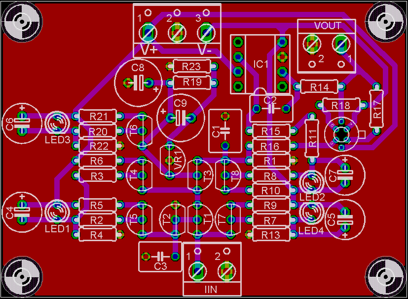
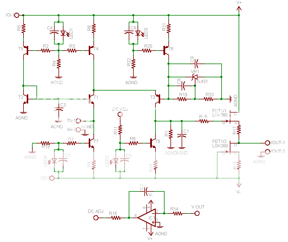
I thought I would post my schematic for a discrete I/V converter for use on the output of an audio DAC here, to see if anyone had any comments or suggestions as to how I could improve it.

This is a discrete open loop DC coupled folded cascode common base amplifier, which steers the current output of a DAC through a pair of common base amplifiers, first an NPN, which is followed by a PNP folded cascode, which, among other things, acts as a level shifter, to get the DC output near ground. Adding an inverting opamp integrator to act as a servo by modulating the CCS of the cascode transistor, a DC coupled output should be relatively easy to realize. This current is then converted to a voltage by R1, in the same fashion as the resistor dump passive I/V solution some people are in favor of, but without the massive loading of the output of the DAC, and all of the problems that entail.

Input impedance depends on IC of the input transistor, which I intend to run at 10mA, so should be about 2-3ohm. BJTs will most likely be 2SC2240BL/2SA970BL parts, due to their extremely high hFE which remains quite linear with regards to IC for the values of IC I am interested in, as well as the low noise and capacitance of this part. Actually I am really using it because that is what Jocko Homo, whose postings have had the greatest influence on this schematic, suggested, and I havnt been able to find any other transistors which look as good.

I plan to pair this converter with AD1862N-J DACs, though it will work with other current out designs. I currently own four of these chips, and am somewhat torn between designing the DAC to have true differential outputs by creating an inverted digital signal with a pair of XORs, or doing phase splitting with a differential pair in the analog domain. There are positive and negative aspects to both options, but I am currently leaning towards going completely differential. These chips arnt exactly as cheap as chips
rolleyes.gif
.

Since it is an open loop design, PSRR is a concern, but due to the heavy use of current sources, and the folded cascode topology, I believe that with decent rail regulation and filtration, this will be a non issue.

There are some changes I am currently evaluating for this design. First is the addition of cascodes on all current sources, though this should be most beneficial for the one based around T8, but hey, cascodes are like cookies, you cant just stop at one. I am also contemplating replacing the current base biasing solutions with emitter-followers, connected for base current error correction as shown by Malcolm Hawksford in his paper "Current-Steering Transimpedance Amplifiers for High-Resolution Digital-to-Analogue Converters". Finally, I am thinking about replacing the open loop JFET buffer with a discrete opamp, since the RC low-pass filter will drastically reduce the extreme high frequency output of the DAC, which is the primary reason for the converter being open loop in the first place. If I do this, however, I would be greatly inclined to make this opamp my headphone amplifier, since I dont like the idea of using two opamps in the signal path when unneccessary. By adding a high current discrete buffer, either diamond or some MOSFET topology, after the VAS of the opamp, I could have a very nice headphone amplifier. I dont really care for the idea of having my headphone amp integrated into my DAC, and it presents some issues with how to impliment the volume control, as there really should be a buffer between the I/V resistor and volume attenuator. If I decide on doing the phase splitting in the analog domain however, I will replace this buffer with a differential pair to provide the phase split, which will take care of the need to buffer the output.

I would appreciate any feedback people here can provide (though not globally in the I/V). For those of you who managed to stay awake to this point, thanks for putting up with my rambling. Since it is not specified in the schematic, VR1 is a TL431.

I-V9.png
 
Apr 7, 2007 at 11:55 PM Post #2 of 33
I'm still not convinced that the low-pass filter on an opamp does much given that the gain is usually pretty low in the 10+ mhz region where you really need it.

Have you simulated this with parasitics? Try feeding signals in the 20-50 mhz range. EDIT: nm the idea I had still requires the negative supply to carry the full noise.

Would be super to keep the noise current out of the supply but I'm not sure that'll even be possible with active I/V.
 
Apr 9, 2007 at 9:25 AM Post #3 of 33
Quote:

Originally Posted by Rescue Toaster /img/forum/go_quote.gif
I'm still not convinced that the low-pass filter on an opamp does much given that the gain is usually pretty low in the 10+ mhz region where you really need it.


Are you referring to an opamp configured as a transimpedance amplifier, using a cap in the feedback loop to reduce HF noise, or are you referring to the low pass filter created by C1 in this circuit not being effective in reducing HF sufficiently? I agree that with a NOS DAC, this would be an issue unless the filter was operating at such a low frequency so as to audibly roll off the highs significantly, but with the OS I plan to use, likely in the form of a SM5847, unless I can get my hands on a PMD100, should let a first order filter be sufficient I think.
Quote:

Have you simulated this with parasitics? Try feeding signals in the 20-50 mhz range. EDIT: nm the idea I had still requires the negative supply to carry the full noise.

Would be super to keep the noise current out of the supply but I'm not sure that'll even be possible with active I/V.


I havnt simulated this, and I dont have any skill with the simulator, so I am afraid the results I would get right now would be worth about the cost I would spend on parts to run the simulation. The other issue with your previous suggestion of replacing the T7 CCS with a resistor is that I think it would significantly increase distortion. My plan is to have this running off it's own regulated supply, somewhere above +/-15v. The folded cascode class A means current draw will truly be constant, which helps us some here. Current draw wont be real high, so a nice ccs fed shunt reg is quite doable to power it.
 
Apr 9, 2007 at 7:01 PM Post #4 of 33
I was referring to your comment on using a discrete opamp for I/V. The slew rate on even multibit converters generates images at full power up to 20 mhz or so, then rolling off around 50mhz. (measurements done on a PCM63). The multibit sigma-deltas are almost certainly faster. Unless your discrete opamp is at least as fast as say, an LM6171 then I'd avoid it.
 
Apr 9, 2007 at 8:53 PM Post #5 of 33
Quote:

Originally Posted by Rescue Toaster /img/forum/go_quote.gif
I was referring to your comment on using a discrete opamp for I/V. The slew rate on even multibit converters generates images at full power up to 20 mhz or so, then rolling off around 50mhz. (measurements done on a PCM63). The multibit sigma-deltas are almost certainly faster. Unless your discrete opamp is at least as fast as say, an LM6171 then I'd avoid it.


Sorry, I wasnt suggesting using a discrete opamp for I/V, but for the output buffer, to replace the JFET buffer seen in the schematic. It would probably be a JFET input, with low gain in the input pair, folded cascode VAS, and I am undecided between MOSFET or BJT output. The whole opamp is likely to be complimentary. The whole point of this open loop discrete design is to prevent the issues present when using an opamp for I/V conversion. This discrete opamp would come after R16 in the circuit, so would be operating with voltage input that has been already filtered. Anyways, the AD1862N-J I have is a multibit R2R DAC.
 
Apr 10, 2007 at 1:14 AM Post #6 of 33
Indeed I like it. Opamps are just fine for basic amplification they only really become an issue in I/V. Although looking at the complexity of the I/V circuit it would be a waste to go so far with that many components and then just flop an opamp on the output.

Plus you don't get the bragging rights of being all discrete
very_evil_smiley.gif
 
Apr 10, 2007 at 1:45 AM Post #7 of 33
Quote:

Originally Posted by Garbz /img/forum/go_quote.gif
Indeed I like it. Opamps are just fine for basic amplification they only really become an issue in I/V. Although looking at the complexity of the I/V circuit it would be a waste to go so far with that many components and then just flop an opamp on the output.

Plus you don't get the bragging rights of being all discrete
very_evil_smiley.gif


I wasnt talking about using a monolithic opamp as a buffer, but instead a discrete one. The only monolithic opamp here will be the servo. Those all discrete bragging rights are quite important too, and contribute greatly to the sound quality, kind of like how those big VTEC stickers add 3-5hp when applied to a car.

Component count is rather high with this, with nearly 50 parts per channel.
 
Apr 10, 2007 at 1:59 AM Post #8 of 33
I think you need to make sure to spec in shiny parts as that's good for at least an extra 15 of dynamic range, -10db of THD+N, and 1200 audiophile points.
 
Apr 10, 2007 at 7:32 AM Post #9 of 33
Did a quick PCB layout for this board, to see how it would work out. This will really be integrated onto the same PCB as the DAC, but I wanted to do a separate board as well. This would work fine for upgrading a current current out DAC. It would be pretty easy to change this to use SMD parts, at least partially. None of the smd transistors I have found are nearly as good for this purpose as TO-92 parts such as 2SC2240BL/2SA970BL. 1206 resistors can easily replace the current through hole parts and some of the caps can be replaced by SMD ones, but I dont really see it being too much of a benefit to do this, unless I really need to shrink the board. It currently measures 69.85x50.80mm, or 2.75x2", and this is only a single channel. Bit bigger than just an opamp, eh? The actual signal path is pretty short; most of the board is taken up by the current sources, biasing parts, and servo.

I-Vpcb.png
 
Apr 10, 2007 at 2:42 PM Post #10 of 33
Good job. Yeah, I would NOT change transistors. The SMD for the resistors would be OK, and would save some space. Some suggestions:

1) IOUT and VOUT connectors should be flipped so that the lock tab is towards the inside of the board.

2) I might flip the LEDs and their associated caps to put the caps towards the board inside.

3) Have you considered doing a 2 channel board with a single power connection? Might be more useful and mono...

Chris
 
Apr 10, 2007 at 3:50 PM Post #11 of 33
Quote:

Originally Posted by Pars /img/forum/go_quote.gif
Good job. Yeah, I would NOT change transistors. The SMD for the resistors would be OK, and would save some space. Some suggestions:


I actually have to change the transistor package I used for this board, because last night when I did the layout, I forgot that I was using a CBE transistor package instead of the necessary ECB, which wont work quite as nicely for the layout because of the collector being in the center of the package, but shouldnt be too hard of a change to make, and will be well worth it.
Quote:

1) IOUT and VOUT connectors should be flipped so that the lock tab is towards the inside of the board.


Yeah, I should, though there is no IOUT connector; I suspect you mean IIN. This is a very simple change to make.
Quote:

2) I might flip the LEDs and their associated caps to put the caps towards the board inside.


I see your reasoning for this, because of board parasitics, and while I dont really feel there will be any real difference in the performance, will look at doing this.
Quote:

3) Have you considered doing a 2 channel board with a single power connection? Might be more useful and mono...

Chris


I hadnt really thought about doing this, because I hadnt been planning to actually build this separate from an integrated DAC. I could and likely would do that if I was intending it for use in modding existing hardware, but I currently have no current out sources, so no need for it. This board would actually be pretty easy to build p2p on protoboard, with everything but ground assembled using just the component legs bent flat and soldered to each pad, and a star ground with insulated wire. Nevertheless, I will see what I can come up with in the way of a dual board if there is any interest, or if I get bored.

I would especially like to get some opinions on the output buffer. Do you guys feel the current open loop FET buffer is the better solution, or should I go for a discrete opamp? I dont really see a good way of implementing a volume control before the buffer that wouldnt have interaction problems with the I/V resistor and low pass filter, unless I accepted that it could only be used fully differentially, and implemented something similar to what Nelson Pass did in his D1 DAC. If I put a simple buffer before a normal style volume pot, then I would prefer to just move the whole opamp/volume control to a separate box, implement a PIC controlled 8 bit relay based attenuator, and let the amp be my headphone amp, and able to take multiple input sources. I would prefer to keep it at least somewhat modular so I can upgrade different components (DAC, pre/headamp, power amp).
 
Apr 10, 2007 at 6:16 PM Post #12 of 33
Interesting project. I like what I see.


Besides already having the parts on hand, is there another reason why you are using the AD1862? It is an older obsolete part currently on Last Time buy status. Just wondering if this soon to be gone chip is special.
 
Apr 11, 2007 at 6:52 PM Post #13 of 33
Quote:

Originally Posted by AndrewFischer /img/forum/go_quote.gif
Interesting project. I like what I see.


Besides already having the parts on hand, is there another reason why you are using the AD1862? It is an older obsolete part currently on Last Time buy status. Just wondering if this soon to be gone chip is special.


I am using the AD1862 because it is supposed to be pretty much the best sounding DAC I can get my hands on. This isnt like people saying the TDA1543 sounds great, even though it measures poorly; the AD1862 is supposed to be something special on all levels. Sure, it is only 20bit, but I have no music recorded that high, or even above 16bit. Apparently, the reason it is discontinued (have fun finding some) was due to an extremely expensive manufacturing process, and Analog wasnt able to sell enough of them to be worth it. In some ways, it is supposed to outperform the PCM1704K, which is pretty much the only other DAC I was thinking about for this project. Either way, both are extremely good R2R DACs.
 
Apr 11, 2007 at 7:50 PM Post #14 of 33
Quote:

Originally Posted by cetoole /img/forum/go_quote.gif
I am using the AD1862 because it is supposed to be pretty much the best sounding DAC I can get my hands on. ... Either way, both are extremely good R2R DACs.


Yeah the specs are darn good. I've got a few DVDs with Linear PCM 2-channel audio.
I'm not sure if any of them are 24-bit. My receiver tells me the sampling rate but not the bits per sample.

In any case I doubt I'll use a AD1862 for my next DAC since as you pointed out they are hard to find.

Digikey has the PCM1704K for a mere $30, but it is not recommended for new designs. <sigh>
 
Apr 11, 2007 at 9:40 PM Post #15 of 33
I actually have a AD1862 DAC made by AA that I have been trying to find a discrete I/V+filter to replace the OPA275's. It has the PMD-100 with the -6db done in that analog domain at the low-pass filter after I/V so it makes it a little tricky to find a drop-in solution.

Cetoole I have the complete schematics for this DAC if you are interested I can email them to you.
 

Users who are viewing this thread

Back
Top