cetoole
1000+ Head-Fier
- Joined
- Nov 28, 2004
- Posts
- 1,271
- Likes
- 11
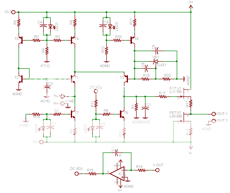
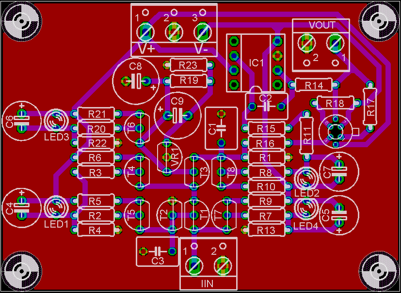
I thought I would post my schematic for a discrete I/V converter for use on the output of an audio DAC here, to see if anyone had any comments or suggestions as to how I could improve it.
This is a discrete open loop DC coupled folded cascode common base amplifier, which steers the current output of a DAC through a pair of common base amplifiers, first an NPN, which is followed by a PNP folded cascode, which, among other things, acts as a level shifter, to get the DC output near ground. Adding an inverting opamp integrator to act as a servo by modulating the CCS of the cascode transistor, a DC coupled output should be relatively easy to realize. This current is then converted to a voltage by R1, in the same fashion as the resistor dump passive I/V solution some people are in favor of, but without the massive loading of the output of the DAC, and all of the problems that entail.
Input impedance depends on IC of the input transistor, which I intend to run at 10mA, so should be about 2-3ohm. BJTs will most likely be 2SC2240BL/2SA970BL parts, due to their extremely high hFE which remains quite linear with regards to IC for the values of IC I am interested in, as well as the low noise and capacitance of this part. Actually I am really using it because that is what Jocko Homo, whose postings have had the greatest influence on this schematic, suggested, and I havnt been able to find any other transistors which look as good.
I plan to pair this converter with AD1862N-J DACs, though it will work with other current out designs. I currently own four of these chips, and am somewhat torn between designing the DAC to have true differential outputs by creating an inverted digital signal with a pair of XORs, or doing phase splitting with a differential pair in the analog domain. There are positive and negative aspects to both options, but I am currently leaning towards going completely differential. These chips arnt exactly as cheap as chips
 .
.
Since it is an open loop design, PSRR is a concern, but due to the heavy use of current sources, and the folded cascode topology, I believe that with decent rail regulation and filtration, this will be a non issue.
There are some changes I am currently evaluating for this design. First is the addition of cascodes on all current sources, though this should be most beneficial for the one based around T8, but hey, cascodes are like cookies, you cant just stop at one. I am also contemplating replacing the current base biasing solutions with emitter-followers, connected for base current error correction as shown by Malcolm Hawksford in his paper "Current-Steering Transimpedance Amplifiers for High-Resolution Digital-to-Analogue Converters". Finally, I am thinking about replacing the open loop JFET buffer with a discrete opamp, since the RC low-pass filter will drastically reduce the extreme high frequency output of the DAC, which is the primary reason for the converter being open loop in the first place. If I do this, however, I would be greatly inclined to make this opamp my headphone amplifier, since I dont like the idea of using two opamps in the signal path when unneccessary. By adding a high current discrete buffer, either diamond or some MOSFET topology, after the VAS of the opamp, I could have a very nice headphone amplifier. I dont really care for the idea of having my headphone amp integrated into my DAC, and it presents some issues with how to impliment the volume control, as there really should be a buffer between the I/V resistor and volume attenuator. If I decide on doing the phase splitting in the analog domain however, I will replace this buffer with a differential pair to provide the phase split, which will take care of the need to buffer the output.
I would appreciate any feedback people here can provide (though not globally in the I/V). For those of you who managed to stay awake to this point, thanks for putting up with my rambling. Since it is not specified in the schematic, VR1 is a TL431.

This is a discrete open loop DC coupled folded cascode common base amplifier, which steers the current output of a DAC through a pair of common base amplifiers, first an NPN, which is followed by a PNP folded cascode, which, among other things, acts as a level shifter, to get the DC output near ground. Adding an inverting opamp integrator to act as a servo by modulating the CCS of the cascode transistor, a DC coupled output should be relatively easy to realize. This current is then converted to a voltage by R1, in the same fashion as the resistor dump passive I/V solution some people are in favor of, but without the massive loading of the output of the DAC, and all of the problems that entail.
Input impedance depends on IC of the input transistor, which I intend to run at 10mA, so should be about 2-3ohm. BJTs will most likely be 2SC2240BL/2SA970BL parts, due to their extremely high hFE which remains quite linear with regards to IC for the values of IC I am interested in, as well as the low noise and capacitance of this part. Actually I am really using it because that is what Jocko Homo, whose postings have had the greatest influence on this schematic, suggested, and I havnt been able to find any other transistors which look as good.
I plan to pair this converter with AD1862N-J DACs, though it will work with other current out designs. I currently own four of these chips, and am somewhat torn between designing the DAC to have true differential outputs by creating an inverted digital signal with a pair of XORs, or doing phase splitting with a differential pair in the analog domain. There are positive and negative aspects to both options, but I am currently leaning towards going completely differential. These chips arnt exactly as cheap as chips

Since it is an open loop design, PSRR is a concern, but due to the heavy use of current sources, and the folded cascode topology, I believe that with decent rail regulation and filtration, this will be a non issue.
There are some changes I am currently evaluating for this design. First is the addition of cascodes on all current sources, though this should be most beneficial for the one based around T8, but hey, cascodes are like cookies, you cant just stop at one. I am also contemplating replacing the current base biasing solutions with emitter-followers, connected for base current error correction as shown by Malcolm Hawksford in his paper "Current-Steering Transimpedance Amplifiers for High-Resolution Digital-to-Analogue Converters". Finally, I am thinking about replacing the open loop JFET buffer with a discrete opamp, since the RC low-pass filter will drastically reduce the extreme high frequency output of the DAC, which is the primary reason for the converter being open loop in the first place. If I do this, however, I would be greatly inclined to make this opamp my headphone amplifier, since I dont like the idea of using two opamps in the signal path when unneccessary. By adding a high current discrete buffer, either diamond or some MOSFET topology, after the VAS of the opamp, I could have a very nice headphone amplifier. I dont really care for the idea of having my headphone amp integrated into my DAC, and it presents some issues with how to impliment the volume control, as there really should be a buffer between the I/V resistor and volume attenuator. If I decide on doing the phase splitting in the analog domain however, I will replace this buffer with a differential pair to provide the phase split, which will take care of the need to buffer the output.
I would appreciate any feedback people here can provide (though not globally in the I/V). For those of you who managed to stay awake to this point, thanks for putting up with my rambling. Since it is not specified in the schematic, VR1 is a TL431.


