New SMD take on the Mint, redesigned PCB
Oct 2, 2005 at 12:10 PM Post #46 of 84
I'm going to dive in from left field.

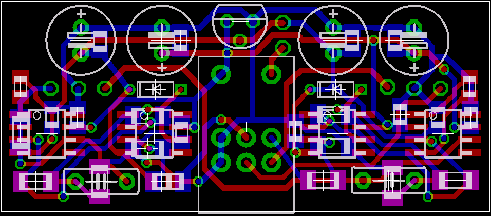
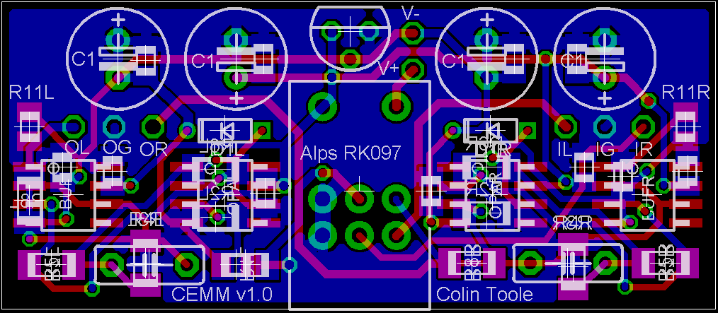
Looking at the layout I think I perceive a bit of the tail wagging the dog going on. Your layout seems to be overly worried about the physical beauty of the positioning of the devices, to the detriment of the routing. First up the symmetric layout of the two channels - you are making a rod for your own back. Also the precise grid lined layout - similar. In crafting a layout that is so space constrained these are luxuries you can't afford.

I would suggest that now you have an existence proof - i.e. you know it is feasible you tear it up and start out like this:

Take a single channel - and lay it out. Don't put borders around the layout yet, just try to lay out one channel in as neat a manner as you can. Don't glue the ICs down as your first pass, sit back and think about the interconnections around them. Attach the local components first, than look to the relative position of the ICs. You might find rotating one 180 degrees helps, or 90 degrees. Currently it looks as if holding them in place has forced all sorts of sub-optimal layout.

Once you have a complete channel, see how you can use it as a building block. You can flow other parts about them. The PS does not need to be a symmetric thing at the top of the board. Nothing says the rail splitter has to sit in pride of place in the middle. I will bet that a ground channel will fit easily, and with much neater layout.
 
Oct 5, 2005 at 7:50 AM Post #47 of 84
Francis, I can see where you are coming from on the layout, and I appriciate the feedback, but I am cureous, what kind of differences would I hear with a better layout than what I have now? I see that some of these traces are longer than they might ideally be, but considering the size of this board, "long" traces are all still well under 3cm, and few are even approaching this length. All components that I wanted to see on this board are present, and excluding the amplified ground channel, which would increase current draw by close to 50%, everything that people here asked for is included. If you can convince me that any layout changes I can do will have any audible impact, or point out traces that you see which could be routed more efficiently, I am all earsm and will gladly break out the ripup tool, but I think this layout should satisfy the goals I had for this amp.
 
Oct 5, 2005 at 7:55 AM Post #48 of 84
finish your work and go to bed now!!!! and this project does not count as your work
biggrin.gif
 
Oct 5, 2005 at 8:03 AM Post #49 of 84
Quote:

Originally Posted by grandenigma1
finish your work and go to bed now!!!! and this project does not count as your work
biggrin.gif


redface.gif
I have been caught, but would you believe me if I said I was writing my paper right now, instead of attempting new layouts in Eagle? I mean, come on, who would work on PCB design when they can write about "A Raisin in the Sun", or sleep?
confused.gif
 
Oct 5, 2005 at 8:35 AM Post #50 of 84
Quote:

Originally Posted by cetoole
but I am cureous, what kind of differences would I hear with a better layout than what I have now? I see that some of these traces are longer than they might ideally be, but considering the size of this board, "long" traces are all still well under 3cm


Hard to say specifically, but one thing that you must consider is the very high frequency performance of the op-amps and buffers typically used in this design. Every trace brings with it inductance. I was particularly worried by the long traces to and from the bandwidth limiting caps. That isn't a solution that guarantees stability to my eyes anyway.

The multi-loop topology has more than its fair share of places where an additional bit of mess can lead to instability, and it may be very difficult to diagnose. Perhaps only manifesting itself as a general feeling that the circuit never seems to sound quite as good as other implementations.

And of course being a geeky DIY design one would expect an excruciating desire to wring the best possible performance out of it
600smile.gif
 
Oct 5, 2005 at 8:36 AM Post #51 of 84
Quote:

Originally Posted by cetoole
Francis, I can see where you are coming from on the layout, and I appriciate the feedback, but I am cureous, what kind of differences would I hear with a better layout than what I have now? I see that some of these traces are longer than they might ideally be, but considering the size of this board, "long" traces are all still well under 3cm, and few are even approaching this length. All components that I wanted to see on this board are present, and excluding the amplified ground channel, which would increase current draw by close to 50%, everything that people here asked for is included. If you can convince me that any layout changes I can do will have any audible impact, or point out traces that you see which could be routed more efficiently, I am all earsm and will gladly break out the ripup tool, but I think this layout should satisfy the goals I had for this amp.


Here is Tangent's response to a similar question:
Quote:

This isn't just a prettiness argument. Sloppy layouts often indicate sloppy thinking. There's a point in a good layout where it feels tight as a drum: moving anything even a little bit has widespread effects on the layout because everything is balanced carefully against everything else. This is a good thing: it means you have balanced the forces as well as you can given the constraints you have.


Oct 5, 2005 at 9:02 PM Post #52 of 84
Quote:

Originally Posted by Francis_Vaughan
Hard to say specifically, but one thing that you must consider is the very high frequency performance of the op-amps and buffers typically used in this design. Every trace brings with it inductance. I was particularly worried by the long traces to and from the bandwidth limiting caps. That isn't a solution that guarantees stability to my eyes anyway.

The multi-loop topology has more than its fair share of places where an additional bit of mess can lead to instability, and it may be very difficult to diagnose. Perhaps only manifesting itself as a general feeling that the circuit never seems to sound quite as good as other implementations.

And of course being a geeky DIY design one would expect an excruciating desire to wring the best possible performance out of it
600smile.gif


Stability, that is a good point, and I too am not happy with how the bandwidth limiting is. Maybe if I rotate R3 and R4, I can put a through hole device straddling it, I will see if it can fit. Do you think the layout would really cause audible differences, or is it mainly stability we are concerned with?

dsavitsk: Sloppy thinking, that is me all right, you should see my room.
biggrin.gif
Any worse in here, and I wont be able to find the bed or the computer, and I at one point lost a Guzzler USB DAC kit in here for a couple months. That said, there are many traces that I cant move at all without changing half a dozen others at this point, while other areas are kinda flexable.
 
Oct 6, 2005 at 7:17 AM Post #53 of 84
Did some work on the board again, tried to take in mind some of the suggestions you had Francis, and I am more pleased with how the layout is now. I also got an Eagle Library file e-mailed to me that had the correct RK-097 object, so you see that added now, sure made routing more difficult. As you can see, the opamp bandwidth limiting cap no longer uses 0805 SMDs with long traces, there is now a rather largish thru-hole cap straddling R3 and R4, so much less parasitic capacitance there, and part selection should be a bit easier. I also changed the CRDs from SOT23 to the standard DO-35 parts, suprisingly to me, not only could I get them to fit better, they made routing much easier. Should I add pads to bypass the power supply caps directly?
cemmbeta11.png


I also found that with some minor tweaking, a groundplane is fully possible, let me know if this is beneficial for an amp like this.
cemmbeta11-groundplaned.png
 
Oct 6, 2005 at 8:20 AM Post #54 of 84
It does look a lot better. After this I think it becomes a more a matter of taste how you add things.

As to the ground plane, my personal, and my no means expert at all feeling, is not to. In this design it is much less clear exactly what ground means, and there is probably more scope to get into trouble than it might avoid. Others might feel otherwise. There is often a bit of difference of opinion here.

You might like to have a look over at the thread building a new version of the PCM2702 DAC board. There may well be some synergy to see whether the boards can be made to physically work together. I suspect quite a few people would be interested in such a pairing.
 
Oct 6, 2005 at 12:06 PM Post #55 of 84
Quote:

Originally Posted by Francis_Vaughan
It does look a lot better. After this I think it becomes a more a matter of taste how you add things.

As to the ground plane, my personal, and my no means expert at all feeling, is not to. In this design it is much less clear exactly what ground means, and there is probably more scope to get into trouble than it might avoid. Others might feel otherwise. There is often a bit of difference of opinion here.

You might like to have a look over at the thread building a new version of the PCM2702 DAC board. There may well be some synergy to see whether the boards can be made to physically work together. I suspect quite a few people would be interested in such a pairing.


Thanks, I'm glad you approve. I see what you mean about ground being kind of uncertain, and while I am relatively sure the groundplaned version would be fine, I kinda prefer the origional grounding more. I have been following the PCM2702 DAC thread lately, and it is very interesting looking, if all power was to be derived from usb or wall power, a DAC board and amp should fit in the smallest Hammond case no problems. Since usb gives us 500mA at 5v to work with, I believe, we should have plenty of current to power the DAC board, and use a DC-DC converter and good regulation to power an amp off the same usb supply. It might not measure quite as well as battery power, but it would be a lot smaller, lighter, and, in my opinion, a great laptop companion for music on the go.
 
Oct 6, 2005 at 1:04 PM Post #56 of 84
Just be aware that you cannot connect the DAC and a MINT directly. MINT uses a virtual ground, while the DAC's ground is 0V.

You should read this thread

Quote:

Originally Posted by Tangent
I recommend you leave the TLE off the MINT board entirely, and construct a new studly vground supply on a separate board. Then you run the MINT from the off-board vground.


icon10.gif
icon10.gif
icon10.gif
icon10.gif
icon10.gif
icon10.gif
icon10.gif
icon10.gif
 
Oct 6, 2005 at 2:49 PM Post #57 of 84
Ah yes! Good point.
biggrin.gif
(From someone listening to his PPA V2 as he types.)

There are possibly a number of ways of solving the PS issue. Since it seems apparent that revisiting PS design is the next in line for the DAC thread, perhaps enough flexibility can be included in the options. An appropriate choice of DC-DC converter(s) may be the appropriate answer.
 
Oct 6, 2005 at 3:39 PM Post #58 of 84
If a dc-dc converter was used on the DAC board, to step the 5v USB power up to 12v or so, then run through an LDO regulator, and wired to the battery inputs of the amp, there shouldnt be any problems at all, right? We would be using the stepped up usb power instead of a battery for the mint, and there would be no need to replace the TLE2426 at all. What Tangent seems to be talking about requiring something more studly than the TLE is powering the mint from a wallwart, wiring the vground to the DAC 0v ground, and the positive rail to the DAC positive rail, which will greatly increase the current that needs to be handled by the TLE, but if we are looking to go the other way, amp powered from the DAC, there should be no such problems, as the TLE only has to handle the current requirements of the Mint. Mouser also stocks 5v to +/-5v regulated DC-DC converters, but they are rather largish, and not cheap, about $12. Sizewize, these two boards come in at right around 50mm x 78mm, or just small enough without batteries to fit in the smallest Hammond. With the Amp at the front of the case, and the DAC at the back, it should be quite simple to also add the option to power both from a single supply wallwart, add a switched jack or diode based system to power the system from the wall when available, or switch to usb power for all other times.
 
Oct 6, 2005 at 5:22 PM Post #59 of 84
The DAC's output ground is connected to 0V. The DAC's 0V becomes MINT's V-. MINT's input ground is connected to the virtual ground. Therefore connecting DAC's output ground to MINT's input ground shortcuts MINT's virtual ground to MINT's V-. You need to do something about this.
 
Oct 6, 2005 at 10:07 PM Post #60 of 84
Quote:

Originally Posted by cetoole
If a dc-dc converter was used on the DAC board, to step the 5v USB power up to 12v or so....


Done. Check out the DAC thread for the updated schematic.
 

Users who are viewing this thread

Back
Top