New SMD take on the Mint, redesigned PCB
Sep 12, 2005 at 6:50 AM Thread Starter Post #1 of 84

cetoole

1000+ Head-Fier
Joined
Nov 28, 2004
Posts
1,271
Likes
11
Well, my friend Eric (cire), and I both love the Mint design, but there are a few things that we have been wanting to be slightly different, a more compact board done in almost all SMD, one that would fit perfectly across the front of the smallest hammond, and leave room for one to stuff 8xAAA batteries in behind it. We also wanted to board mount the Alps RK097 switched potentiometer, to give the amp a simpler front panel and retain good performance. We also decided to go with 2 single channel opamps, to allow the use of various high end opamps, such as the OPA627. R8 has been pulled out of the feedback loop, making it simply an impedance adapter, with a trace between the pads that must be cut to enable it. This amp is the first PCB layout work that both Eric and I have done, and definitly the most complex electronics work we have tackled, so there are likely to be some errors. Eventually, we plan to get some boards made up for ourselves, probably at Sparkfun simply for economic reasons (we are both students). We removed all the things we didnt need, LED, diode, input caps, buffer bandwidth resistor, crds, but once we feel that the design is good, we will likely add the CRDs back in, and add opamp bypass capacitors.

Anyway, here is the current layout, done in the freeware version of Eagle. If anyone wants the board files, for any reason, just shoot either one of us a PM, we will be more than happy to provide them, honored even
etysmile.gif
.

CEMMBeta.jpg


This layout is a work in progress, there will be updates following.
Colin
 
Sep 12, 2005 at 6:53 AM Post #2 of 84
please please put bandwidth compensation caps we can use the design with fast opamps (eg the ths4631)

and if you were to do that, I'd be VERY interested in building one of these..
 
Sep 12, 2005 at 8:56 AM Post #3 of 84
Don’t use the autorouter, it does a terrible job

1206 smd sizes are much easier to work with than what looks like 0603 from here

The general layout could be improved heaps, I wouldn’t be trying to stick to the original mint layout of the resistors, rearrange it for a better layout suited to the smd components, and if needed you could mount parts either side of the board

Bypass the opamp and buffer pins with ceramics as close to the power pins as possible

Ground planes are also good, just if you do it may be wise to have a hole in the ground plane around the input pins of the opamps to keep stray capacitance low
 
Sep 12, 2005 at 10:28 PM Post #4 of 84
no autorouter was used. the routing by hand really wasnt that hard.

yes, 0603 is being used, Colin suggested 1206 a few days ago, but i said no, since we'll need to increase the depth of the board by quite a bit. i dont have one of those Hammonds, so i'll ask him to measure how much more PCB space can be used and still able to fix 8xAAA.

ground planes may be good, but i havent figured out how to do that yet. same goes for putting components on the other side.

how much of a sonic difference would the layout make? its not a highspeed circuit, so i wouldnt think much.
 
Sep 12, 2005 at 10:44 PM Post #5 of 84
Quote:

Originally Posted by cire
ground planes may be good, but i havent figured out how to do that yet. same goes for putting components on the other side.

how much of a sonic difference would the layout make? its not a highspeed circuit, so i wouldnt think much.


1) draw a polygon in Eagle with "Isolate" set to a low value, and name it the same as your ground trace. It will automatically fill the correct area, while isolating the pins that aren't grounded according to the set parameter. Be careful of stray capacitance around the opamps inputs.

2) Use the "MIRROR" command to flip the part over to the other side

3) Layout makes ALL the difference! The circuit for our purposes is not high speed, ie we only need the first 20kHz, but remember that the opamps are specced well in to the 10s or even 100s of MHz, so you must take into account their behaviour at those high frequencies. The way they are behaving at 1MHz will influence how they behave simultaneously at 1kHz

4) 0603 isn't significantly harder to solder, but make sure you get small (>= 26awg) solder and a good pair of tweezers. Also, make sure you have a very small tip and a low power soldering iron; components that size don't take much heat
wink.gif
 
Sep 12, 2005 at 10:54 PM Post #6 of 84
A few more things;

1) Run DRC, some of those traces look less than a hair off the other parts. Set the grid resolution higher if need be

2) The outline of the board should be done in Layer 20 (Dimension) with width set to zero. I'm not sure, but I think the CAM processor would not handle it properly otherwise.

3) Get rid of as many vias as you can, they may appear to make the layout easier, but in fact all they show is that the layout is not optimal. I suspect you'll need a few, but certainly not as many. Dakiller's advice is sound in not copying the resistor layout directly from the MINT, SMD needs a different approach.

4) Back to the 0603, R8 cannot be 0603; the maximum dissipation is 1/16th of a watt. In the R8 position you'll need at least 0805 (1/8th watt)

5) Don't use 90 degree corners, they make the layout more awkward and (some say, although I can't say I notice) alter the sound. However, changing to 45 degrees has the advantage of making the layout easier as you can router corners more closely
 
Sep 12, 2005 at 11:35 PM Post #8 of 84
Nice start.

Is this really that much smaller than the existing mint when it's cut in half and stacked?

Not trying to thread crap, but not sure using SMD resistors is really saving that much room in your layout. Try having them mounted on the top and bottom of the PCB, that should save you more room, and is one of the main benefits of using SMD resistors.

The addition of being able to use dual single channel OP amps is a nice touch. Might be a good idea to allow some jumpering to be able to use a single dual channel OP amp like the AD8620.

-Ed
 
Sep 13, 2005 at 4:36 AM Post #9 of 84
i would move the chips and traces further north towards the cap and you could have room for larger resistors.
 
Sep 13, 2005 at 7:44 AM Post #10 of 84
nobody suggested yet, so I'll do it - do the schematics first in schematics editor and then switch to the layout editor.. all the leads will be connected together by 'airwires' so that you can't possibly make a mistake and also you will only lay out the devices and then use Route command instead of Wire to change from airwires to regular tracks.. all the tracks will adapt to the pitch of the particular component.. look at your opamps and their pads and then the tracks going from them..
 
Sep 13, 2005 at 9:07 AM Post #11 of 84
Any thought of using the space savings to add space for a fully buffered ground? That would be a pretty amazing, ultra-high-end piece of audio equipment on a piece of real estate that you could swallow if the secret police caught up with you.
 
Sep 13, 2005 at 1:48 PM Post #12 of 84
Quote:

Originally Posted by Dougigs
Any thought of using the space savings to add space for a fully buffered ground? That would be a pretty amazing, ultra-high-end piece of audio equipment on a piece of real estate that you could swallow if the secret police caught up with you.


That would essentially wind up being a Pimeta... not a bad idea... do a Pimeta in the space of a MINT
 
Sep 13, 2005 at 3:59 PM Post #13 of 84
Jazper: That looks simple enough, I will just add holes for some small film caps to parallel R4, as stated by Tangent on his "Working with Cranky Op-Amps" page. Probably put spacing for the nice WIMA MKS-2 5mm caps on to parallel R4.

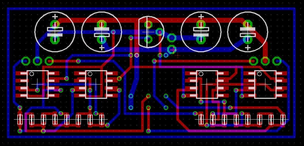
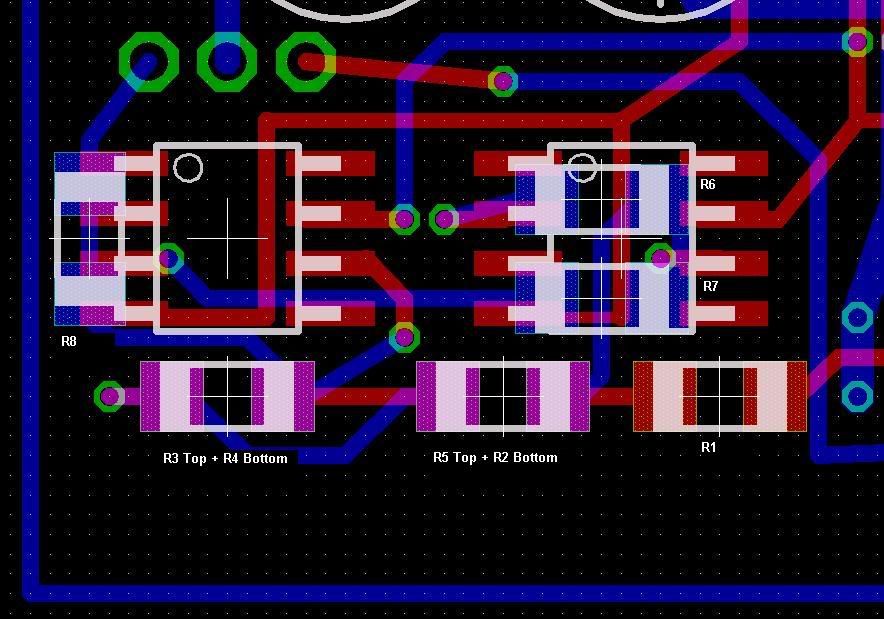
DaKi][er: As cire said, no autorouter was used, and I do believe we will step up to 1206 smd resistors all around, get some of those nice Vishay's. I had been contemplating changing the resistor layout before (and changed R8L as you can see), so I think we will go ahead and do that, hopefully tomorrow, as I have class until 10:30 tonight. We had been planning on bypassing the opamps, rail-ground, and while we hadnt thought about doing the same for the buffers, there is no reason not to, ceramics are cheap. I dunno if a ground plane is in this amp's future though, as we are most likely to put most of the resistors on the back of the board. Maybe a groundplane in all areas except for the resistor network?

Guzzler: Makes sense about the layout making a difference, especially in opamp stability. Good point about soldering the 0603 resistors, but I probably would tin the pads first, then reflow holding the resistor on with tweezers. As we now plan to go to 1206, it is kinda a moot point. We will remove as many vias as are viable, but there will definitly have to be some, if for no other reason than because there will be resistors on the back of the board. Are there any points in the amp that it is more important not to have vias?

Sinbios: I think we will stick with 2 single channel opamps, we are using SO8 opamps, so the use of a brown dog adapter isnt really possible, and we cant have too much vertical height in front of the caps, because of the I/O jacks. Also, you can buy most (all?) of the popular opamps in single channel configuration, but there are several (OPA627) that are not made as dual channel opamps.

Edwood: No, not really that much smaller footprint than a split mint, but it is only one board, and the layout is different. A split mint doesnt fit across the front of the smallest Hammond 1455, believe me, I have tried. Once we put the resistors on the back, we will save a little more space, but I dont really expect this to be a smaller board than the split mint. The people here made several good points that the layout is everything, and I cant imagine the additional wiring needed to let people use a dual opamp in this configuration would be good. If you really wanted though, it would be possible to cut all the traces from the opamp on either side, so the pads are isolated from the rest of the board, and air wire it to allow what you want. Wouldnt be pretty, efficient, or easy, and likely wouldnt sound as good, but it is possible.

Skyscraper: Not really any space to move further north, we could get a little, but as there is plenty of room on the back, I think we will just do that.

Glassman: That makes a good deal of sense, I never thought of that, or knew it was possible. I will give it a shot, see what we come up with.

Dougigs: I think we would have to extend the length of the PCB to do that, so would probably have to move up from the 80mm Hammond to 90mm or so. That said, we might try it, but not right now, maybe after we get this working. Also, I only have 2 BUF634U's here, and all the places I know of are out of stock. Maybe they will have more when we are ready to try adding a buffered ground. Maybe if I can find a supply of buffers I will try it, or I might just modify the layout for a buffered ground and post it here for anyone interested (and has buffers) to build.
I would have to look, it may be possible to stuff the third buffer on the back of the pcb, along with the resistors.

A lot of comments, keep them coming, I hope to have a revision up before the end of the week. I am kinda suprised there were no comments about our choice in using 4 electrolytic caps for the psu instead of 2 like Tangent's mint uses, or the complete lack of input caps, led pads, or other stuff. Also, if anyone knows of a battery holder for 8xAAA that fits in the back of the smallest hammond 1455 case, that would be very useful, as right now, I will probably have to do a custom setup that will not be nearly as nice. If we step up to the next length case, we could probably stuff a LM317 based recharging circuit and DC power jack into the amp, and maybe we could fit it, if we made the battery pack as compact as possible, although probably difficult to remove, in the current size.
 
Sep 14, 2005 at 3:44 AM Post #14 of 84
so we got a lot of work to do. the agenda:
1. clean up the layout. make it more efficient and if possible, each channel only uses ones side of traces (major overhaul here)
2. add bypassing (for the op-amps? i'll let Colin clear this up)
3. rig up an 8xAAA battery holder. the prototype of this will be made with duct tape and card board
4. get more buffers. Colin has two left and i've got none.

other things that might be done:
-have pads on both sides for the buffers. stacking buffers without any stacking (genius idea of Colin)
-turn it into a pimeta
-space permitting, adding a charging circuit with a DC jack. we need to find a really tiny jack to pull this off.
 
Sep 14, 2005 at 6:20 AM Post #15 of 84
Did a little work on the resistor layout, sorry it is so hard to see anything. So far, I have just done the left side, wanted to see what you all thought before taking the time for the right channel. Note the 1206 resistors. I might have to move some stuff slightly for decoupling reasons, but nothing much.
CEMMnewresistor.jpg
 

Users who are viewing this thread

Back
Top