dsavitsk
MOT: ECP Audio
- Joined
- Aug 3, 2003
- Posts
- 2,883
- Likes
- 44
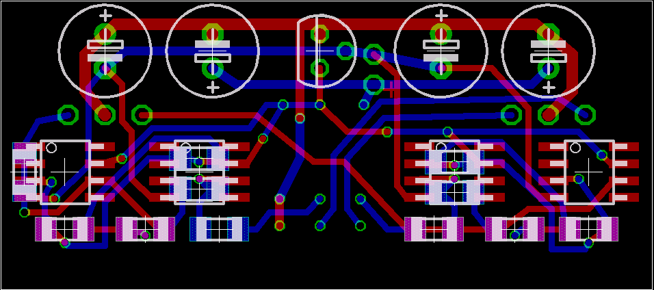
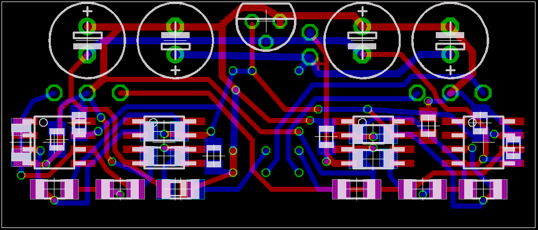
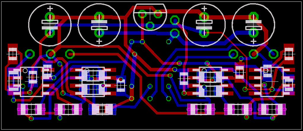
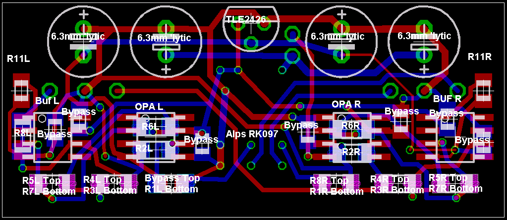
I think the standard advice is to make the angles 45 degrees. It will clean up the layout quite a bit. For an example, follow my own learning progression in this thread: http://www6.head-fi.org/forums/showthread.php?t=130517
-d
-d