


KT88
500+ Head-Fier
- Joined
- Nov 7, 2004
- Posts
- 948
- Likes
- 26
Quote:
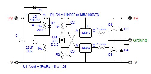
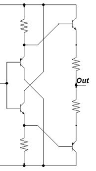
This isn't exactly what I meant. I meant really build it like a class-AB buffer. You should add a resistor from D3 to the positive supply and another one from D4 to the negative supply. This will keep the diodes slightly conducting at all times. It can also be done with BJTs instead of diodes:

But in this case its not really important since what's driving this point is an op-amp so no need for the extra current gain of the first transistors.
You can now also get rid of D1-D2. The bases of the output transistors only have 2 (forward biased) diode drops between them, so the B-E voltages will be well within the allowed voltage range.
Here's the output for this exact circuit with 2.2K for the resistors to the left, and 0.1R resistors at the output. The op-amp used for this simulation is the good old opa134, it can only work with a +-18V supply, so I've used that value and not a +-20V like in the previous sim. Everything is wrapped in feedback of the opamp. Capacitors are just 1uF (due to the very low output impedance there very little need in the capacitance, even lower value could be used) and load amplitude is exactly the same as before:

The feedback drops the output resistance much lower than before.
You can also try that with the LT1097, but it doesn't perform as good in this case (yet still much better than the previous circuit did under the same conditions).
In this case since the feedback to the op-amp is coming from the output directly, using huge caps might hurt the stability. The output resistance of the circuit and the load capacitance add another pole in the loop. It must be kept high enough to maintain stability. This turns out not to be an issue since the very low output resistance is so low there's no real need for the capacitance anyway (and the results back-this up), so just use a small cap and you're fine. It's possible to have large capacitance at the output but than the feedback must be slightly modified to have an alternative path at high frequencies (using a small cap from op-amp out to inverting input + resistor between the inverting input and the vGND node), but it will actually only hurt performance in most cases and requires extra parts/larger caps.
BTW, the reason I didn't post this circuit before is very simple, this is what everybody else do. tangent has an IC buffer in the pimeta, and a discrete (and better performing) buffer in the PPA. So this is simply a simpler implementation of the same thing that everybody else use. The reason I liked the way this thread started is that the circuit didn't use the straight forward way, it had a very strange look to it. Finding new and different ways to do things is always more fun than doing it the "right" way")
Thanks, KT88, but what took you so long? We could have been here about 60 posts back...
w
This isn't exactly what I meant. I meant really build it like a class-AB buffer. You should add a resistor from D3 to the positive supply and another one from D4 to the negative supply. This will keep the diodes slightly conducting at all times. It can also be done with BJTs instead of diodes:
But in this case its not really important since what's driving this point is an op-amp so no need for the extra current gain of the first transistors.
You can now also get rid of D1-D2. The bases of the output transistors only have 2 (forward biased) diode drops between them, so the B-E voltages will be well within the allowed voltage range.
Here's the output for this exact circuit with 2.2K for the resistors to the left, and 0.1R resistors at the output. The op-amp used for this simulation is the good old opa134, it can only work with a +-18V supply, so I've used that value and not a +-20V like in the previous sim. Everything is wrapped in feedback of the opamp. Capacitors are just 1uF (due to the very low output impedance there very little need in the capacitance, even lower value could be used) and load amplitude is exactly the same as before:
The feedback drops the output resistance much lower than before.
You can also try that with the LT1097, but it doesn't perform as good in this case (yet still much better than the previous circuit did under the same conditions).
In this case since the feedback to the op-amp is coming from the output directly, using huge caps might hurt the stability. The output resistance of the circuit and the load capacitance add another pole in the loop. It must be kept high enough to maintain stability. This turns out not to be an issue since the very low output resistance is so low there's no real need for the capacitance anyway (and the results back-this up), so just use a small cap and you're fine. It's possible to have large capacitance at the output but than the feedback must be slightly modified to have an alternative path at high frequencies (using a small cap from op-amp out to inverting input + resistor between the inverting input and the vGND node), but it will actually only hurt performance in most cases and requires extra parts/larger caps.
BTW, the reason I didn't post this circuit before is very simple, this is what everybody else do. tangent has an IC buffer in the pimeta, and a discrete (and better performing) buffer in the PPA. So this is simply a simpler implementation of the same thing that everybody else use. The reason I liked the way this thread started is that the circuit didn't use the straight forward way, it had a very strange look to it. Finding new and different ways to do things is always more fun than doing it the "right" way
")
