Super Nintendo SPDIF, DACs, and You
Feb 19, 2015 at 9:26 PM Post #16 of 32
 
Well I ordered a set of pcbs and 3 sets of components, hooked one all up and I got nothing...

 
Hi GameTechUS,
 
Sorry to hear about the issues you're having with the board, I hope I can help make it work.
 
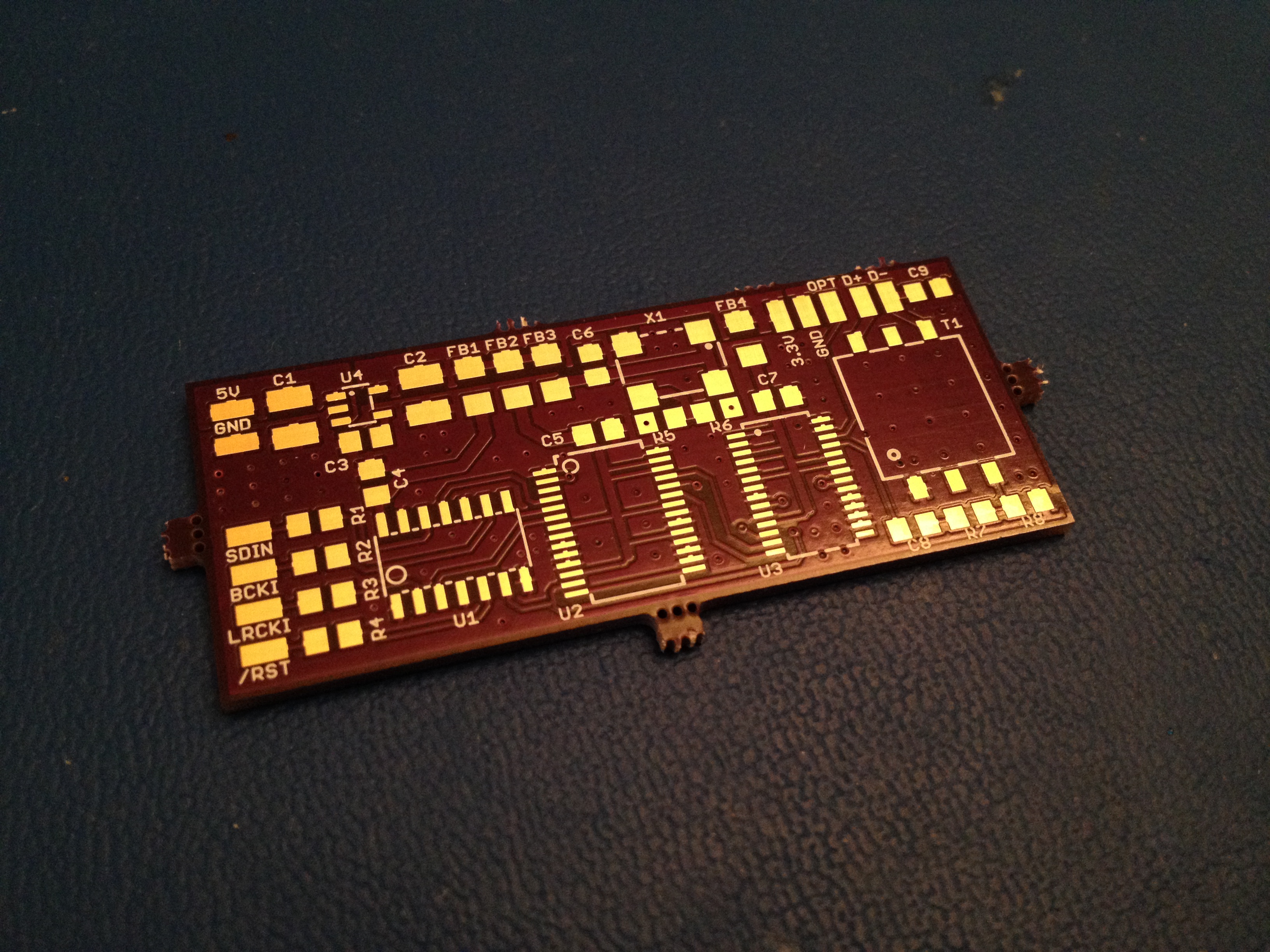
Can you compare your stuffed board to the picture of mine I posted earlier in this thread?  Ensure that all ICs are oriented correctly, especially X1 as that should be oriented upside down with pin 1 in the top right corner when viewing the board right side up.  Also note that FB3 and FB4 are installed horizontally rather than vertically.  
With the power off, check continuity between the positive leg of the bypass capacitor near each IC and the IC's pins that are connected to 3.3V (refer to one of your unpopulated boards or the PCB renders on OSH Park).  If these are okay then check that the regulator is outputting 3.3V by measuring across C2 and check that there's 3.3V across the capacitor near each IC.
 
Check that there's continuity between the left side of R5 and pin 2 on U2, and between the right side of R6 and pin 21 on U3.  If these are okay then the two chips should be getting a master clock signal from the oscillator.
 
Also check the idle current draw of the board alone when powered outside of the SNES, with the /RST pad connected to 5V and nothing connected to SDIN, BCKI, LRCKI, D+, and D-.  If I remember correctly I measured ~25ma during my testing.  If yours is much higher then you might have a short somewhere, if it's lower check that pin 6 on U1 is outputting 3.3V and make sure that pin 13 on U2 and pin 9 on U3 are soldered correctly and have continuity.
 
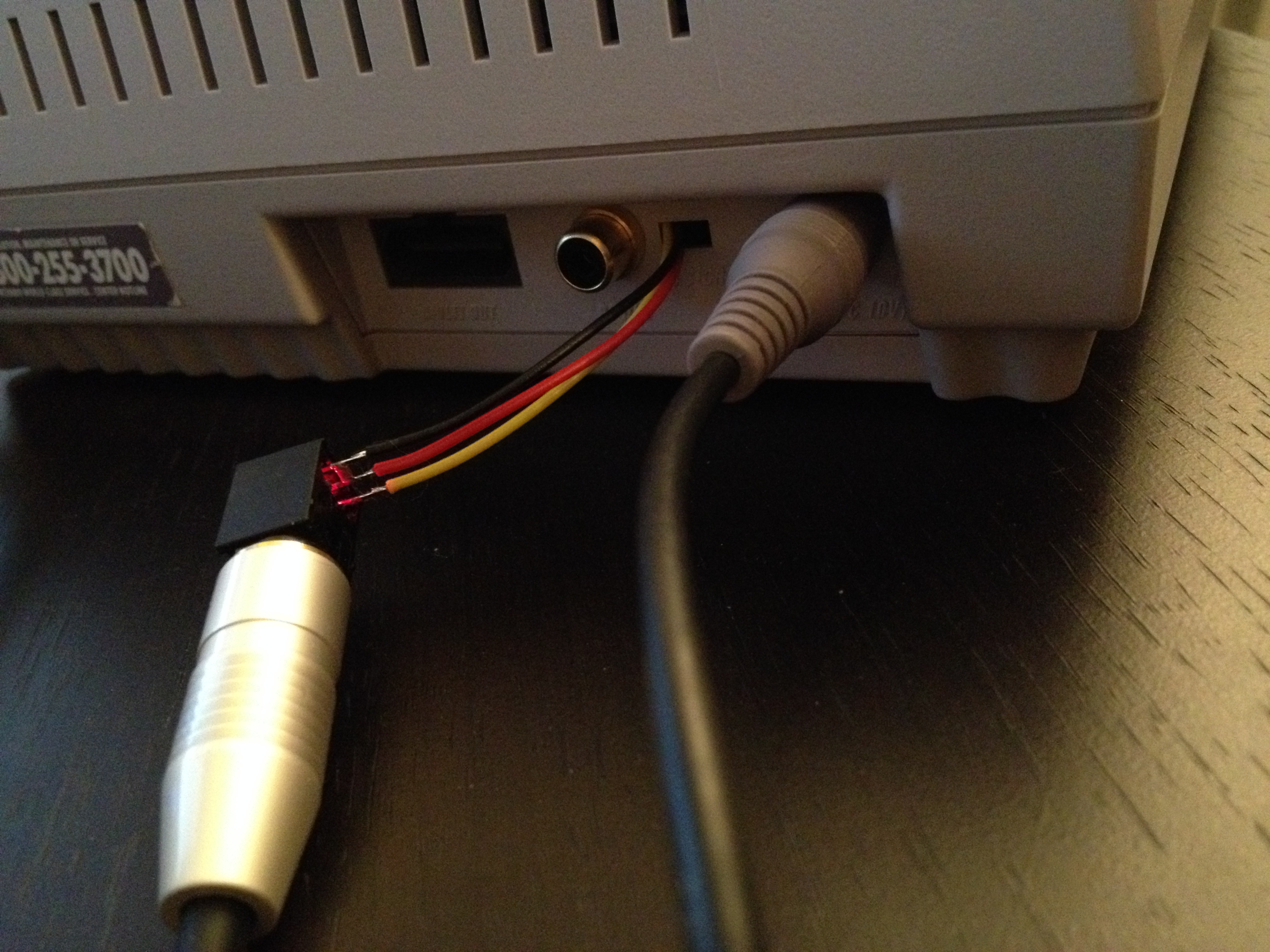
The D+ pad should be connected to the center pin of your RCA jack and D- should be connected to the RCA jack shield.  Don't connect D- or the RCA jack shield to the SNES' ground as that would ruin the isolation the transformer provides.
 
Would you happen to have high resolution pictures of your stuffed board?
 
I appreciate your criticisms of my PCB and will remember them if I decide to release something like this again in the future.
 
L
 
Feb 20, 2015 at 2:55 PM Post #18 of 32
   
Hi GameTechUS,
 
I appreciate your criticisms of my PCB and will remember them if I decide to release something like this again in the future.
 
L

Ok, all seems good now, I hadn't made any mistakes on the pcb stuffing.
I did find I had a different receiver with digital audio in and it seems to work just fine with both this and the simple gamesx mod.
So the KLH was the issue after all and the much older Sony shines...
I should have known!
I'm going to get my buddy Kevtris to really look at the pcb design though and i'll let you know what we come up with.
 
Jun 7, 2015 at 2:57 PM Post #20 of 32
Hi there,
 
I'm really interested in this project and I've got a question.
What modifications would be needed to drive a TOSLINK LED (optical out like this one : picture) and of course keep the RCA jack ?
 
I've already done this mod : http://gamesx.com/wiki/doku.php?id=av:snes_sp_dif which drives both but your circuit looks so much more amazing !
 
Thanks !
 
Jun 8, 2015 at 9:02 PM Post #21 of 32
  Hi there,
 
I'm really interested in this project and I've got a question.
What modifications would be needed to drive a TOSLINK LED (optical out like this one : picture) and of course keep the RCA jack ?
 
I've already done this mod : http://gamesx.com/wiki/doku.php?id=av:snes_sp_dif which drives both but your circuit looks so much more amazing !
 
Thanks !

Hi,
 
If the simple CS8406 mod from GameSX works with your receiver/DAC then I suggest sticking with that, unless you plan on moving to a receiver/DAC that is stricter with the sample rates it accepts.
 
I had some time last month to work on a slightly updated version of this board with some improvements suggested by GameTechUS in one of his videos, but haven't had the time to build it yet.  Here's a photo:


What has changed is the following:
 
  1. Enabled thermals for all planes for easier solderability
  2. Increased distance between traces and pads on U1
  3. Added a pad for optical output (can be used simultaneously with coaxial output)
  4. Added output pads for the regulated 3.3V and GND (simplifies wiring to the optical transmitter)
  5. Changed digital pulse transformer to the smaller Murata DA101JC (or DA101MC)
  6. Board is now a bit shorter lengthwise, so 3 boards come to $8.70 from OSH Park
 
Hopefully I'll have some time this week or weekend to build it, and if everything goes OK I'll be sure to post again and put it up on OSH Park's Shared Projects so you can order it.
 
L
 
Jun 9, 2015 at 10:45 PM Post #23 of 32
  Hi,
 
This new version looks very good :)
 
Isn't your circuit better than just a CS8406 ? In accuracy I mean, or electronic insulation ?

 
Since my board resamples the audio data it is by nature not bit-perfect compared to the original 32-ish kHz audio stream and is thus less accurate in that sense.  However, any noise and/or distortion added by the SRC4192 is well below that of modern DACs and is by all means transparent.  If you mean accurate in terms of sample rate, then yes, it should be very close to 96 kHz provided you use a high quality oscillator.
 
In terms of electrical isolation you could always add a transformer to the standalone CS8406 circuit and get the same benefit :wink:
 
Jun 11, 2015 at 11:20 PM Post #24 of 32
Success!  Here are some pictures:
 
 
(Note that C3 is not installed because I used a TI LP5907 which does not have a noise reduction pin like the TPS79333)
 
Although this version is easier to solder because of the thermals it's a bit trickier to stuff since you have to be even more strategic with the order you place the parts.
 
Thankfully it works as expected.  Connecting both coaxial and optical to my Denon AVR-2112CI at the same time and switching between the inputs produces the same audio so I trust it's working well.  I'll play some games for a few hours over the next few days and if there are no issues I'll put it up on OSH Park.
 
L
 
Jun 14, 2015 at 6:56 PM Post #27 of 32
Hi all,
 
SNES S/PDIF v1.1 is now up on OSH Park:
 
https://oshpark.com/shared_projects/5NrKCmY9
 
And here's the updated BOM:
 
PartsManufacturer Part #Digi-KeyMouserPackageValueTypeQty
FB1, FB2, FB3, FB4HI1206T500R-10240-2412-1-ND875-HI1206T500R-10R1206  4
C1, C2GRM32ER71A476KE15L490-5312-1-ND81-GRM32ER71A476KE5LC121047uX7R2
C3, C6, C8C0805C103K5RACTU399-1158-1-ND80-C0805C103K5RC08050.01uX7R3
C4, C5, C7, CoptC0805C104J5RACTU399-1171-1-ND80-C0805C104J5RC08050.1uX7R4
C9C0805C220J5GACTU399-1113-1-ND80-C0805C220J5GC080522pC0G/NP01
R1, R2, R3, R4, R5, R6RR1220Q-680-DRR12Q68DCT-ND754-RR1220Q-680DR080568 6
R7RR1220P-2490-D-MRR12P249DCT-ND754-RR1220P-2490D-MR0805249 1
R8RR1220P-111-DRR12P110DCT-ND754-RR1220P-111DR0805110 1
U1SN74LVC125ADR296-8453-1-ND595-SN74LVC125ADRSO14  1
U2SRC4192IDB296-15234-5-ND595-SRC4192IDBSSOP28  1
U3CS8406-CZZ598-1121-5-ND777-CS8406-CZZTSSOP28  1
U4LP5907MFX-3.3/NOPB296-38557-1-ND595-LP5907MFX-3.3NPBSOT23-5  1
U4 (alternative)TPS79333DBVR296-12961-1-ND595-TPS79333DBVRSOT23-5  1
X1C3391-24.576 549-C3391-24.5765x7mm  1
X1 (alternative)FXO-HC736R-24.576631-1186-1-NDXPO-HC736R-24.5765x7mm  1
T1DA101JC 580-DA101JC   1
T1 (alternative)DA102MC811-2663-ND580-DA102MC   1
Optical TransmitterPLT133/T10W1080-1430-ND638-PLT133T10W   1
 
There were a few changes to the BOM:
  1. Changed U4 to the ultra-low noise TI LP5907
  2. Changed X1 (and the X1 alternative) to more stable 25ppm parts
  3. Changed T1 to the smaller Murata DA100/DA100J series
  4. Added alternatives for U4, X1, and T1
  5. Added an optical transmitter and the decoupling capacitor for the transmitter, Copt
  6. Added part numbers for Mouser
 
A few notes for the parts/stuffing:
  1. If the LP5907 is used for U4, leave C3 unpopulated
  2. If the TPS79333 is used for U4, populate C3
  3. The pin out of the PLT133/T10W optical transmitter is incorrect in the datasheet: when looking at the transmitter from the bottom with the back toward you, the order of the pins is actually Vin, Vcc, GND
  4. If the optical transmitter is air wired, the Copt surface mount capacitor fits perfectly between the Vcc and GND pins
  5. Take your time and think of the order in which you stuff the board.  I started with X1 and worked outwards, and didn't run into any issues.  Be sure to:
    1. Install U2 and U3 before installing U1 and T1
    2. Install T1 before installing C8, R7, R8, and C9
    3. Install U4 before installing C1 and C2.
 
Again I make no guarantee that it will work or not blow up your system, but if you run into any issues I'm glad to help.
 
L
 
Aug 13, 2015 at 4:30 AM Post #28 of 32
Well I ordered a set of pcbs and 3 sets of components, hooked one all up and I got nothing...
I'm a disappointed with documentation here as well.
For instance i'm not sure how exactly d+ and d- are supposed to be used.
I'm going to coax if that helps.


Hey how's it going GameTechUS .... I ran across this S/PDIF project from one of your YouTube Videos and Kev also mentioned you so that's how I located your YouTube channel was through him.
Anyhow...
In about 2005/2006-ish, I installed the S/PDIF mod that was shown on alpha-II website. It was a very simple circuit and I did notice that the digital audio didn't sound as well as the analog R/L outputs native to the SNES. While I can deal with that, what bothered me the most was the volume level was not as loud as the analog R/L outputs. As a result, I don't really use the S/PDIF mod.
I ended up installing all the circuitry for that mod inside the metal RF modulator box inside the SNES, and used it's existing RCA jack so the console looks completely unmodified.

I just ordered 3 of the boards from OSH Pk... I saw the parts list and numbers from L-Train in an above post from him.

So basically now what I need is a wiring diagram of where to connect the wires from the board to the SNES mainboard... It has been way too long since
I installed the original S/PDIF mod and I won't really remember.

In your above post you mentioned some disappointment in the documentation, so I was wondering what documentation IS out there or what you might have.
'Cos I can't seem to locate documentation at all.

Any help would be greatly appreciated.
 
Aug 13, 2015 at 10:47 PM Post #29 of 32
Any help would be greatly appreciated.

 
Hi hbo3,
 
Here's a run-down of the pads on the SNES S/PDIF board and what to connect where:
 
  1. 5V is the 5V power input to the board.  Connect this to the output pin of the SNES' 7805 voltage regulator.  I believe this is labelled "O" on the SNES' PCB.
  2. GND is the ground pad of the board coming from the power supply.  Connect this to the ground pin of the SNES' 7805 voltage regulator.  I believe this is labelled "G" on the SNES' PCB.
  3. Read Alpha-II's page to determine the type of APU you have.  Then use the following table to match the SNES S/PDIF pad to the correct pin based on your APU.  The pin numbers are labelled in regular intervals on the SNES PCB so they're easy to find, but they're only labelled every 10 or so.  It's very easy to solder to the wrong pin so just remember to count twice and solder once :wink:
    SNES S/PDIF padDescriptionS-DSP pinS-APU pin
    SDINSample data input4493
    BCKISample clock input4292
    LRCKILeft/right clock input4394
    /RSTReset4716​
  4. 3.3V, GND, and OPT are the 3.3V output, ground, and optical S/PDIF output pads.  Refer to your optical transmitter's data sheet to connect these pins correctly.  For example, the PLT133/T10W part I specify has pins called Vcc, GND, and Vin, connect these directly to the 3.3V, GND, and OPT pads on the SNES S/PDIF board, respectively.
  5. D+ and D- are the coaxial S/PDIF output pads.  If you're using an RCA jack for coaxial output, connect D+ directly to the center pin and D- directly to the shield.  Do not connect D- to the SNES' ground as that would not give you the benefit of galvanic isolation via the transformer.
 
The SNES appears to output audio at a maximum of -6 dBFS which would explain why it sounds so low, it's effectively half volume relative to the maximum your DAC can output.  My mod won't help that, it will still output at maximum -6 dBFS.  The volume/loudness of the SNES through a digital audio mod relies entirely on your DAC and how much voltage it outputs at full scale.
 
If you have any more questions please don't hesitate to ask!
 
Sep 2, 2015 at 11:07 AM Post #30 of 32
Just discovered that you shared a v1.1 circuit on OSHPark!  Going to give assembling the V1.1 circuit a try.  Hopefully it will turn out better than the V1.0!
 
I noticed that you're using TXN for the coaxial output?  Why is that?  Won't it be out of phase/inverted?  It looks like the TXN is actually routed to the isolated D- connection (inverting the inverted output)?  Please elaborate on the design choice.
basshead.gif


Users who are viewing this thread

Back
Top