PPA v2 Project Announcement
Jan 26, 2005 at 10:12 AM Post #92 of 106
Quote:

Originally Posted by morsel

BrownDog adapters are relatively cheap


I read about this recommendation of not using IC sockets in one of those Jim Williams app. notes that ppl referred me to.

My whole PPA v1 board has no sockets. I hand-test each IC and screen for above-average parts before soldering it onto the board.

Could we please restore those SOIC-8 pads underneath the DIP-8 socket?
 
Jan 26, 2005 at 12:10 PM Post #93 of 106
The TRIAD output circuit in this PPA 2.0 Version comprises a novel dc bias circuit, which comprises an enhanced complementary fully symmetrical current mirror to provide an Ultra bias boosting circuit for biasing the Driver and output transistors. This Sophisticated Bias arrangement makes the charging rate faster than the discharging rate for each respective half of the complementary Diamond Buffer output stage. The Complementary current Mirrors set the quiescent current of the driver and output transistors. This dc bias circuit comprises an adjustable JFET Constant Current source supplying a precise amount of DC current to both Positive and negative current mirror circuits at the same time and in precisely equal amounts. Each complementary current mirror simply mirrors the Current supplied by the Jfet Current source in precisely equal amounts and assures that each PNP and NPN half of the diamond buffer is supplied with exactly the same amount of current. This maintains True complementary handling of the Audio waveform so as to completely remove crossover distortion regardless of whether or not the load current is greater than the standing bias current,
Thus, we have a Ultra stable bias circuit capable of charging and discharging the Driver and output transistors with a charging rate faster than a discharging rate.

In a conventionally biased class AB amplifier, the average bias supply current increases as power increases. This increased average current results in an increased voltage drop in the resistive part of the bias circuit. This in turn reduces the average voltage drop across the forward-biased PN junction of the power-amplifying transistors, pushing the amplifier into class B operation Therefore, the output will be saturated as the output further increases in response to the Audio signal.

Linearity and efficiency are two contradictory requirements in a power amplifier. The tradeoff between the linearity and efficiency are the classic design dilemmas for the power amplifier designer. Therefore, This Buffer Topology is designed to provide a power amplifier circuit with a novel biasing scheme, which is simple but capable of maintaining good control of quiescent current for the power transistors.

By properly controlling current the output Transistors, the charging and discharging rates can provide the ideal bias current for achieving optimum Current gain and extended Bandwidth in the Output stage.

In this unique Bias Circuit, the jfet current source bias generates the bias current simultaneously to each complementary Wilder current mirror circuit to establish the drive current to each respective half of the diamond buffer. Thus only one current source is needed to control the quiescent current of Both PNP and NPN Driver and output transistors and eliminates the unequal bias currents of each half of the Diamond buffer that would result if two conventional current sources are employed like in the Jung style diamond buffers.

The most linear method of implementing a current mirror is to use a 1:1 ratio, thus 1 mA produced by the Jfet Bias generator results in 1 Ma output for the Current mirrors. In this manner thermal tracking of the Mirror is maintained without matched transistors since the power dissipation in each of the mirror transistors are the same thus the ultra Vbe of all 4-mirror transistor will remain constant.

For battery operation, the availability of current sources that operate accuratly in a low voltage environment is very desirable so as to obtain the most available voltage swing for a given supply voltage. A current mirror circuit will typically operate up to the saturation point of the Mirror transistors. This allows the output to swing to within 1 volt or less of the supply rails while still maintaining adequate bias current to maintain low distortion even at output levels approaching Clipping.

While more complex in design and requiring more component parts than a conventional Diamond buffer, the enormous benefits derived from applying Bias current in symmetric fashion to each half of the Diamond Buffer Circuit results in the ability to slew at very high rates and still retain a symmetrical rising and descending slew rates. This is very desirable to eliminate odd order distortion components known to result from improperly or asymmetrically biased Complementary output stages. The result over the use of two separate independent conventional current sources is a more smooth yet detailed reproduction of textures. Musical Peaks are presented clearly yet never thrown in an uncontrolled manor out at the listener. Control with detail and micro dynamics is just a few of the benefits that result by using this more complex “Ultra Bias” method of biasing a complementary output stage. Additional advantages are ultra low DC offset and an extremely high current gain resulting in high input impedance with equal input bias currents and thus make this buffer also suitable as a stand-alone Unity gain Headphone driver that will maintain its low DC offset even when the source resistance is quite high. This lends itself to use as a stand-alone Buffer that will allow you to build the PPA without any op amps and related support circuits. By simply jumpering the op amp non-inverting input to the output and not installing the op amp casscode constant current sources your PPA can be a unity gain feedback free headphone amp with an all discrete component signal path.

Different designers have quite different views on just want qualities are desirable in an Amp and thus you see quite different topologies coming from different designers. I designed this Circuit to obtain the absolute best performance and IMHO the best sound quality available in a battery operated easily transportable headphone Amp. If you desire class A or something else this amp is not I suggest you build one of the other many fine Amplifiers available online and not try to make the PPA 2.0 into something it is not intended to be, However I believe the PPA 2.0 will hold its own against any of the top quality Headphone Amps available, But of course IM Biased.
basshead.gif
 
Jan 26, 2005 at 4:58 PM Post #94 of 106
Quote:

Originally Posted by ppl
By simply jumpering the op amp non-inverting input to the output and not installing the op amp casscode constant current sources your PPA can be a unity gain feedback free headphone amp with an all discrete component signal path.


This diamond buffer is a very exciting development.

I've been wondering this question for weeks, holding off on asking it, it crystalized thinking about this buffer: Given the merits of this buffer, would it make sense to build an active power supply, using two LTZ1000 IC voltage references as described on "Art of Electronics" p. 341 to step down an 18 volt source to +,- 7.2V and virtual ground, then use these as inputs into three diamond buffers?

To be clear, such an amp would have six diamond buffers, 3 for the power supply, 3 for audio out. The "raw" power supply would feed the power diamond buffers, the power diamond buffers would feed the audio out diamond buffers.

It seems that the only issue that PPAv2 doesn't address, that a newbie like me could fantasize about having in an amp, is a power supply impervious to voltage variations caused by the output buffer loads. Throwing a ton of caps at the problem is a dog very successfully chasing its tail, we're still always exponentially decaying toward where we want to be, only at a very fast rate. An active power supply could just jump to where it wants to be, faster.

This reminds me of control theory, old fashioned methods for balancing a stick on your nose work no better than a person constantly adjusting, the stick is never exactly vertical. Modern digital control mechanisms can perfectly right the stick in finite time. It's still an unstable equilibrium, outside interference can require further control, but it's much better.

It would seem to me that caps are old-fashioned, an active circuit would be much better, obliviating differences between botique and jellybean power caps, and shrinking headamp height requirements. Of course, I'm a newbie just speculating here, but I'd love to read your answer.

Edit: I've moved my question to its own thread, "Active" power supply using PPL's diamond buffer?
 
Jan 26, 2005 at 5:16 PM Post #95 of 106
Nice writeup, PPL.

Syzygies: a dual power supply defeats the purpose of using virtual ground. Read about it in old PPA design threads, or at the websites.

Quote:

I read about this recommendation of not using IC sockets in one of those Jim Williams app. notes that ppl referred me to.

My whole PPA v1 board has no sockets. I hand-test each IC and screen for above-average parts before soldering it onto the board.

Could we please restore those SOIC-8 pads underneath the DIP-8 socket?


Development is closed, myhui. You would have to convince Tangent and PPL to respond to your request. Here is my take, in the cold cruel light of day. You are going to unnecessary and painful extremes for little real world benefit. Sockets are convenient and don't affect the performance of the amp in any way that you can hear or measure. If we were to restore the so8 pads the traces would parallel each other to arrive at their final pins due to the requirement of orienting the so8 pads sideways on the underside of the board to fit between the dip pads. It's not as if the layout would be optimized for the sole use of so8 pads. Given that, you might as well use the BrownDog adapters and allow yourself the ability to try other opamps down the road.

attachment.php
 
Jan 26, 2005 at 8:22 PM Post #98 of 106
Quote:

Originally Posted by jamont
Has the prototype been tested with OPA637 in L/R channels?


I tested mine with OPA637 at a gain of 20dB works great. it also is stable with the much more finicky AD8065. The reasons for previous stability were from not optimizing the amp feedback to take into account the different transfer function of the IC vs discrete buffer. By reducing the Inner loop gain by changing R6 from 1 meg to 470K we reduce the inner loop gain and thus the feedback factor.

In addition the op amp to buffer input isolating resistors are changed from 1K to 2.2K to accommodate the dramatic increase in input impedance if the new buffer.

As those of you with an in depth understanding of feedback networks know the wider the bandwidth of the gain stage the less feedback factor can be supported and maintain stability. Ever notice that High Speed op amps most often have lower open loop gain than your typical op amp 60-70dB as opposed to over 120db For the typical precision types. The opa637 is the exception to this however if you look at the opa637's gain vs phase plot you’ll notice that this device has almost no gain/phase margin and if one were to go by the plot on the data sheet it would appear the opa637 should not be stable at all even on its own.

Syzygies> the concepts you talk about while conceptually intriguing are not applicable for the small form factor of the PPA. Please remember that this is a portable Amp and space is limited. I cannot imagine where you’re going to put 3 more buffers at on the ppa board. I believe that with the power supply rejection ratio provided by the ground channel and the Jfet rail isolation network. I cannot see how you consider that we addressed this issue with massive capacitance since the PPA actually use substantially smaller capacitance that other premium Amps. However thanks for taking the time to look into this and comment upon it for us hear.
 
Jan 26, 2005 at 11:44 PM Post #99 of 106
Quote:

Originally Posted by ppl
The TRIAD output circuit in this PPA 2.0 Version comprises a novel dc bias circuit, which comprises an enhanced complementary fully symmetrical current mirror to provide an Ultra bias boosting circuit for biasing the Driver and output transistors. (etc., etc.)


Great explanation of the circuit, PPL! Thanks again for your and the rest of the team's hard work on this project. From an electronics industry insider's point of view, this kind of collaborative, open development is extraordinarily rare and very refreshing. The kind of results that come from your work are more typical of a closed, proprietary shop - from a commercial organization, not from a group of enthusiasts that are more interested in giving back to their community than making a zillion bucks. Beyond the fact that you've created what is sure to be a great amplifier, you've also demonstrated incredible altruism.

BRAVO!

-Drew
 
Jan 27, 2005 at 1:12 AM Post #100 of 106
Quote:

Originally Posted by drewd
Great explanation of the circuit, PPL! Thanks again for your and the rest of the team's hard work on this project. From an electronics industry insider's point of view, this kind of collaborative, open development is extraordinarily rare and very refreshing. The kind of results that come from your work are more typical of a closed, proprietary shop - from a commercial organization, not from a group of enthusiasts that are more interested in giving back to their community than making a zillion bucks. Beyond the fact that you've created what is sure to be a great amplifier, you've also demonstrated incredible altruism.

BRAVO!

-Drew


Thanks for your Kind words. I truly believe in the free exchange of Knowledge. However some don't see this as a virtue. my Grandpa one sed Don't let Phil mind the store because he will give it away
eek.gif
To this day i try and remain true to my Virtues.

Credit also is Due to Morsel who did the PCB layout and as you all know Tangent for his time and monetary investment to bring these projects to the Light of Day and publishes the most in depth how to sections available on the WWW. In addition Credit is also due to AMB for his 2Cents.Real practical guy that AMB is for sure.
 
Feb 1, 2005 at 9:27 AM Post #101 of 106
Are the components and their values settled ? I recognized that e.g. R1 changed from 4.32k (PPA v1) to 4k. I don't mind that 4.00k is not available since the next value 4.02k is only 0.5% away. Just wondered whether the values are still under optimisation.

Which transistors (in addition to the complement pairs) should be matched ? Can you give hints how many are probably needed to find a good match among them ? I got no clue how far production varies and how close they should be matched to achieve good results.
 
Feb 1, 2005 at 4:43 PM Post #102 of 106
No, the values have not been settled. The 4K .vs. 4.32K discrepency between my schematic and Tangent's schematic is of no real consequence and reflects the theoretical nature of the values I recorded. We never did as thorough a resistor choosing process as I would have liked, trusting that it would all come out in the wash, but most people just used the values we suggested, and we let the matter slide. After the PPA v2 production prototype arrives and is tested we will hopefully update the parts values.

You can probably get away without matching transistors and still achieve good results.
 
Feb 2, 2005 at 7:57 AM Post #103 of 106
I chose 4.32K and 3.32K simply because they're exactly 1K apart (R5) and because one of the two values at least is common. With 4.02K, you go with 3.01K as the mate, and neither is a common value.
 
Feb 23, 2005 at 9:04 AM Post #104 of 106
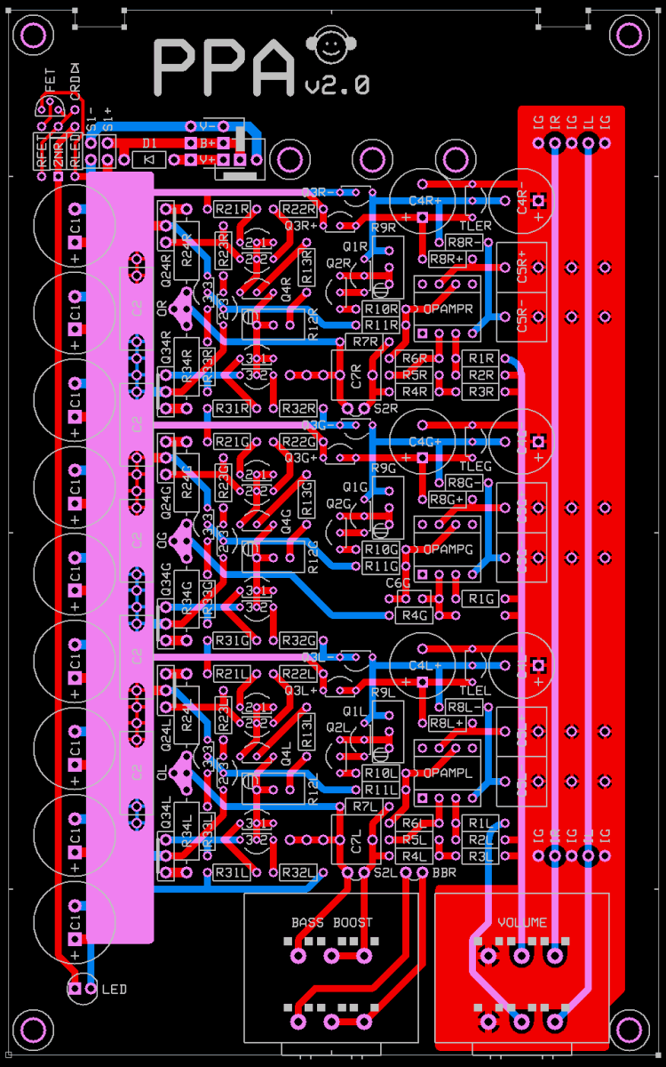
A few last minute changes prompted by the final production prototype:

All capacitors and related pads now have 35mil holes to accommodate .8mm leads.
R2, R6 changed from 1M to 470K. C6G changed from 10pF to 33pF.

ppa.gif


ppasch.gif
 

Users who are viewing this thread

Back
Top