My first DIY questions -CMoy- (picts)

Mar 22, 2009 at 2:47 PM Post #31 of 49
That's well cool, you could fade them in and out. :P

xx
 
Mar 22, 2009 at 4:21 PM Post #32 of 49
Hmm does not sound that bad, though
biggrin.gif
 
Mar 22, 2009 at 7:05 PM Post #33 of 49
You have a very very nice proto-board there.
I built mine on this kind of board too.
Don't worry about bridging one point to another. One tip I use is to tin the two points you intend to join, then supply generous amounts of solder while you shuffle the iron between the two joints. It'll bridge very easily... sometimes too easily, which tends to end up in frustrating unintentional shorts to surrounding components when you're not careful.

And since I wasn't able to follow tangent's layout exclusively thanks to single-only opamps I had (OPA627), I had to be pretty luxurious with my own layout (and since I was using redundantly gigantic caps too).

I did everything point to point as per schematic and it worked pretty well.
DSC00316small.jpg

If you were to look at the brown-ish rail-splitter circuitry I added after the whole build, you can have an idea of what the rest of the circuit looks like underneath.

If you wish, I can take a pic of the underside too, but it's quite a mess and I doubt it'd help. LOL

If it's your first time, ignore miniaturization to prevent confusing yourself.

Good luck.
 
Mar 22, 2009 at 8:09 PM Post #34 of 49
ph33lix, thanks a lot for your help.

If you do not mind I would appreciate to see the underside of the board.
Then for using a single op-amp, did you follow the schematics for one op-amp, and you "expanded" it in order to fir two sockets in?

With the wires and capacitors (massive ones indeed) I cannot see the configuration.


Thanks again.
 
Mar 23, 2009 at 4:30 PM Post #35 of 49
Quote:

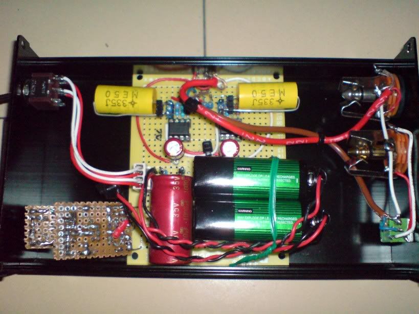
Originally Posted by ph33lix /img/forum/go_quote.gif
You have a very very nice proto-board there.
I built mine on this kind of board too.
Don't worry about bridging one point to another. One tip I use is to tin the two points you intend to join, then supply generous amounts of solder while you shuffle the iron between the two joints. It'll bridge very easily... sometimes too easily, which tends to end up in frustrating unintentional shorts to surrounding components when you're not careful.

If you wish, I can take a pic of the underside too, but it's quite a mess and I doubt it'd help. LOL


Well today I started. Damn my fingers hurt a bit from touching the sucking wire -works good sometimes even too good and sucks the metal fast-

Trying to bridge one point to another was indeed impossible... And in some of the points if I put a big blob over the holes then I could not pass any metal through them, as they were covered.

I should start with the jumpers first, no? In order to follow the same type of board.

Oh and I'd really appreciate a pict of the underside of your build.

Guess I am going to give it another try, plus I will have to return soon to get more soldering iron
smily_headphones1.gif
 
Mar 23, 2009 at 5:43 PM Post #36 of 49
Quote:

Originally Posted by Bullseye /img/forum/go_quote.gif
Well today I started. Damn my fingers hurt a bit from touching the sucking wire -works good sometimes even too good and sucks the metal fast-

Trying to bridge one point to another was indeed impossible... And in some of the points if I put a big blob over the holes then I could not pass any metal through them, as they were covered.

I should start with the jumpers first, no? In order to follow the same type of board.

Oh and I'd really appreciate a pict of the underside of your build.

Guess I am going to give it another try, plus I will have to return soon to get more soldering iron
smily_headphones1.gif


Yeah, you can lay down the jumpers first to set the circuit up for the components.
There's no fixed working style and this is probably a good circuit to kick start a system that will work for you.

Sorry, was at work all day and just took pics... just hold on.
 
Mar 23, 2009 at 6:05 PM Post #37 of 49
http://i6.photobucket.com/albums/y21...y/DSC00394.jpg
This is the underside. The bottom portion is the money shot, that's where the signal path, opamps and stuff are. You can see that there are lots of "used" pads to the top left corner, that was the result of numerous ****ups with the power supply... because the opamp (I used the OPA627 which tangent DID warn was quite a difficult bugger) kept throwing the virtual ground 6v down the negative rail whenever I plugged in low impedance headphones.

http://i6.photobucket.com/albums/y21...y/DSC00395.jpg
Top side if you were to flip the board from left to right. You can see that each channel was simply a mirror of each other and the audio in/out portion placed in the middle.
The smaller Elna Cerafine electrolytics are output caps that I put in as extra to block any outcoming DC... just in case. With or without didn't sound much different to me anyway, so I went for safety.

http://i6.photobucket.com/albums/y21...y/DSC00396.jpg
Underside of the virtual ground circuit. The TLE->OPA->BUF buffered feedback virtual ground thing you can find in the tangentsoft site.

http://i6.photobucket.com/albums/y21...y/DSC00318.jpg
Topside of said virtual ground rail splitter. Thanks to this, I am getting a very even split of +9.06v and -9.06v when juicing with a pair of 9volt batteries in series. (if you're using one of the more forgiving opamps that tangent talks about on the opamp page, you can ignore this)

-edit-
changed pics to links since they're way huge.
 
Mar 23, 2009 at 7:14 PM Post #38 of 49
thanks for the pictures.

I had to stop due to work, but I put the jumpers, R1 and one C1, then if I am not wrong I should look at the schematics and close the power supply circuit with either wire or solder.

Oh and how can I easily cut a board? I need to cut it in different sizes.
 
Mar 23, 2009 at 7:31 PM Post #39 of 49
Quote:

Originally Posted by Bullseye /img/forum/go_quote.gif
thanks for the pictures.

I had to stop due to work, but I put the jumpers, R1 and one C1, then if I am not wrong I should look at the schematics and close the power supply circuit with either wire or solder.

Oh and how can I easily cut a board? I need to cut it in different sizes.


Shaping is pretty easy.

There's the messy way and there's the clean way.
Messy way involves a bit of sawing if you have a saw. But it's sure-fire and you are less likely to snap off any important sections.
The clean way involves scoring along the holes of where you want to snap off with a utility knife on both sides, holding both sides with a firm grip and then snapping it. It is definitely done best when the board is empty.

You can see that my rail-splitter section was quite hastily snapped to size. :P
 
Mar 24, 2009 at 7:08 PM Post #40 of 49
This is what I have done so far:

dsc00234zrj.jpg

dsc00235akk.jpg

dsc00236qih.jpg


Then when I connect 9V the LED turns on, I am trying (following Tangent's tutorial) to test the power supply, but I wanted to move on and make the rest of the soldering in order to see what connections are missing for the power supply to work.

For today I will stop with it, so I am open to any advice/help with the soldering.
I have not soldered the R5 because I prefer to finish the power supply.

Plus I cut the board (and I did a mess in some parts). I believe they are not any problem for it to work.

Top left side is were I tried to fill the space between the holes to "copy" radio shack's board

EDIT: The op-amp I have done it today, so it is not messy, the top part was my number one attempt
biggrin.gif
 
Mar 24, 2009 at 8:09 PM Post #41 of 49
What you can do to make things easier, especially with the ground plane, is to get a bare solid core hookup wire and solder at the top and bottom. You can then solder whatever needs to be connected to ground to it.

Oh yeah, the I bridge one copper pad to another AFTER I mounted the component. It's very difficult to bridge first and leave the hole open for mounting components like what you tried to do at the top left.
Like for your current state of the build, I see that there are some points that are ready to be bridged right about now.

For example, from the input cap to the resistor leg... just lay your iron across the two pads with solder ready in hand. Once one of the solder points melt (even both would do too), just jab in your solder so that it flows from the melted pad, along your iron and onto the intended pad.

With enough practice, you can do it real quick and easy.
 
Mar 24, 2009 at 8:19 PM Post #42 of 49
Good job bullseye, you're almost there and getting really close!
smile.gif


You're gonna get it going very soon, just remember the yellow highlights I drew below are supposed
to be wired/soldered together since you don't have the same board as Radio Shack's:

dsc00234zrjcopyi.jpg


Good luck!

zk
 
Mar 24, 2009 at 9:56 PM Post #43 of 49
thnks for the tips, zkool448 & ph33lix

Will do that tomorrow. That is what I was thinking that was missing. I saw the schematics and the circuit was not "closed", however I had my doubts if I had to wire the yellow marks zkool marked in the pict.

Can't wait to finish it, plus ph33lix, what you see on the left side it just the LED and battery clip to test the power supply. Once I finish it and test power supply and amplification part (need alligator clips in order to test that last one) I will put it in my altoids box I have. I have some spares just in case I screw up.

I will also do another ones as I bought enough material to make two. The other C1 @ 220 microFarads are 63V, not 35V as those in the picts, consequently they are bigger. I guess I will have to expand the board in order to make the connections.

There is one thing I don't understand at the moment, and it is what the jumpers do. Are they another way to link to holes together?.

On the yellow part you marked zkool48, why are 3 holes needed to be linked? Is that so that when making the schematic out of those connections everything can be set as in a single line? (basically that is how the schematics are)
 
Mar 24, 2009 at 11:22 PM Post #44 of 49
Quote:

Originally Posted by Bullseye /img/forum/go_quote.gif
There is one thing I don't understand at the moment, and it is what the jumpers do. Are they another way to link to holes together?.


Yes
smile.gif


Quote:

Originally Posted by Bullseye /img/forum/go_quote.gif
On the yellow part you marked zkool48, why are 3 holes needed to be linked? Is that so that when making the schematic out of those connections everything can be set as in a single line? (basically that is how the schematics are)


.. and Yes
smile.gif


zk
 
Mar 25, 2009 at 6:52 AM Post #45 of 49
Bahhh, zkool448 you might want to guide me through with my cmoy too.
smily_headphones1.gif


I'm so bummed right now, I don't know how to bridge my board to the one shown in Tangent.
frown.gif
Not being able to read schematics doesn't help, either.
 

Users who are viewing this thread

Back
Top