cetoole
1000+ Head-Fier
- Joined
- Nov 28, 2004
- Posts
- 1,271
- Likes
- 11
Quote:
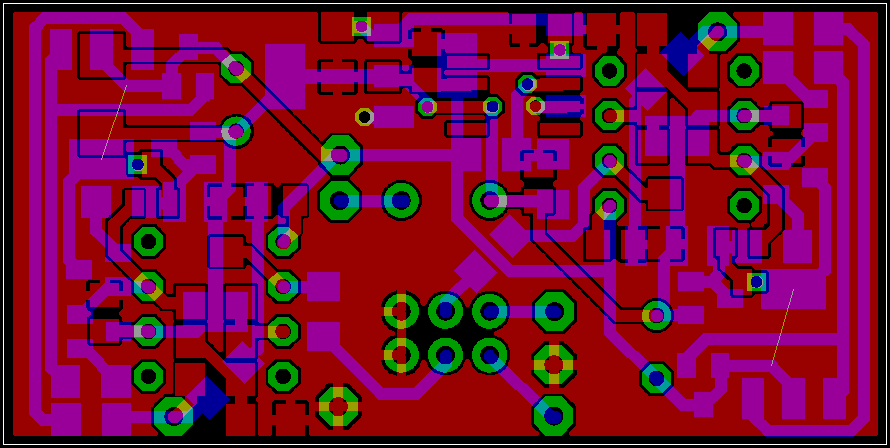
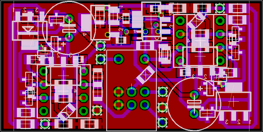
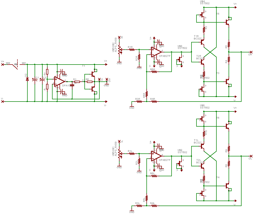
Yes it is, but the eagle parts library doesnt have that part, and I havnt made one up yet. I assume the best way of representing that part would be as a jfet with the Source and Gate shorted?
Quote:
No idea, thats why I am trying it out, and if its terrible, the transistors can be omitted, resistors shorted, and a high current opamp, like the OPA551u, of which I have several, can be substituted. I would like to, as much as possible, get away from using the parts we have now that have only one source, and a lot of availability problems, and I couldnt make another class AB buffer fit on the board without increasing size.
Quote:
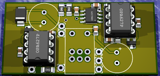
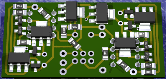
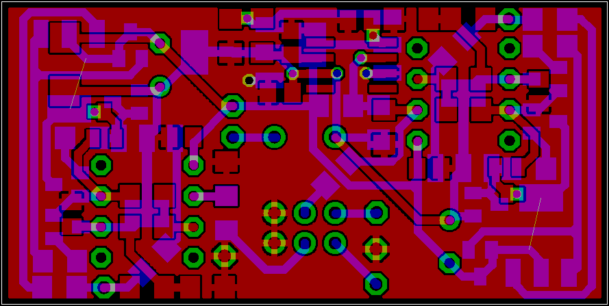
I dont think of it as finalized, the first prototypes have just been ordered. I figure as much of my mistakes might exist in the orientation of the sot23 transistors as anything, although linked schematics and parts will help mitigate this. Also on that prototype order were pcbs for a diamond buffer board very similar to the one on this amp, just with jfet ccs instead of crds, and TO92 transistors and axial resistors that I will try using in a similar multiloop design (pimeta).
| Originally Posted by peranders It's an advantage if you use the correct symbols. It saves a lot of confusion. |
Yes it is, but the eagle parts library doesnt have that part, and I havnt made one up yet. I assume the best way of representing that part would be as a jfet with the Source and Gate shorted?
Quote:
| Originally Posted by peranders I saw also that you have a class B virtual ground. You have bypassed a bit but I wonder how good this will be. |
No idea, thats why I am trying it out, and if its terrible, the transistors can be omitted, resistors shorted, and a high current opamp, like the OPA551u, of which I have several, can be substituted. I would like to, as much as possible, get away from using the parts we have now that have only one source, and a lot of availability problems, and I couldnt make another class AB buffer fit on the board without increasing size.
Quote:
| Originally Posted by thedoctor just concerned since there's a few new designs surfacing up in here, and finalized in a few days after initial schematics. |
I dont think of it as finalized, the first prototypes have just been ordered. I figure as much of my mistakes might exist in the orientation of the sot23 transistors as anything, although linked schematics and parts will help mitigate this. Also on that prototype order were pcbs for a diamond buffer board very similar to the one on this amp, just with jfet ccs instead of crds, and TO92 transistors and axial resistors that I will try using in a similar multiloop design (pimeta).