jcx
Headphoneus Supremus
- Joined
- Jul 24, 2002
- Posts
- 2,371
- Likes
- 371
I see some more problems; I hadn’t realized –in was the lower pin, in your layout its trace runs under your +in resistor body – a real no-no, you’ve increased capacitance and loop area of the most critical connection in the circuit; check out the evm layout, the feedback resistor should be right up against the –in pin to minimize cap at the –in node
Likewise the output trace picks up a few(?) pF unwanted parasitic C by running under the bypass cap body before the 10 Ohm isolating resistor that lets the amp handle Cload
You like symmetry, try applying it to pwr! – V+ and V- trace to the tpa have the same “average position” adding a extra 1/r to the mag field attn for balanced current flow
Putting the bypass caps under the tpa on the backside (preferably with the gnd ends near the midline of the tpa) get them out of the way and reduce inductance – 0805 really, really is best here without going to totally unsolderable parts
the 0.1 uF value is really too large for a 100 MHz bandwidth circuit –inductance renders bigger C less useful above the self resonance; 0.1 uF probably have <30 MHz srf, I wouldn’t use anything bigger than 10nF at the op amp pwr pins, maybe 0.1uf near the pwr entry could discourage some AM/CB radio input to the board
my idea:
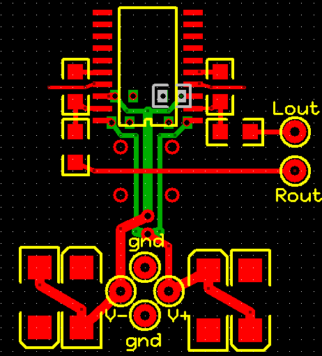
Small green sqs are 0805 caps on backside – big via in pad is bad for automated/reflow soldering but fine for hand soldering – grey is superimposed 0805 outline for reference
I also show 2 pwr input gnds, for any pwr wire length you should consider twisting ea supply w/gnd and twisting the pairs together – or braid
[edit: should short R.L V+ at tpa too, also need to flip/rotate, I started upside down but this shows the ideas]
Likewise the output trace picks up a few(?) pF unwanted parasitic C by running under the bypass cap body before the 10 Ohm isolating resistor that lets the amp handle Cload
You like symmetry, try applying it to pwr! – V+ and V- trace to the tpa have the same “average position” adding a extra 1/r to the mag field attn for balanced current flow
Putting the bypass caps under the tpa on the backside (preferably with the gnd ends near the midline of the tpa) get them out of the way and reduce inductance – 0805 really, really is best here without going to totally unsolderable parts
the 0.1 uF value is really too large for a 100 MHz bandwidth circuit –inductance renders bigger C less useful above the self resonance; 0.1 uF probably have <30 MHz srf, I wouldn’t use anything bigger than 10nF at the op amp pwr pins, maybe 0.1uf near the pwr entry could discourage some AM/CB radio input to the board
my idea:
Small green sqs are 0805 caps on backside – big via in pad is bad for automated/reflow soldering but fine for hand soldering – grey is superimposed 0805 outline for reference
I also show 2 pwr input gnds, for any pwr wire length you should consider twisting ea supply w/gnd and twisting the pairs together – or braid
[edit: should short R.L V+ at tpa too, also need to flip/rotate, I started upside down but this shows the ideas]
