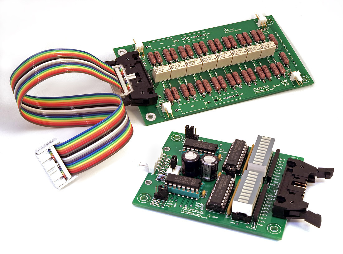
Hot on the heels of the δ1 attenuator, here is the second application module for the LCDuino-1 "system": the δ2 (delta2), a relay-based input/output selector board.
δ2 supports two channels per board, and up to eight ports per channel. Each port can be configured to be either an input port or output port by setting two jumpers. Also, not every port need to be populated. Thus, you can have an arbitrary number of input or output ports, as long as the total number of ports per channel does not exceed eight. This makes the δ2 very flexible, and could be used in a variety of pre-amplifier or headphone amplifier applications.
Similar to the δ1 attenuator, the δ2 board contains a "driver" section and a "selector" section which may optionally be snapped apart and mounted separately. In fact, the "driver" section of the δ1 and δ2 boards is identical.
The δ2 board is also the same size as the δ1, with the same mounting hole and interface/stacking connector locations, so they could all be stacked together and share the I2C bus, power supply and ground connections.
Here is a 3D rendering of the PCB:
The PCB layout (for a larger version
click here):
The schematic diagram is spread over four pages. The first two pages shows the Driver and Selector sections, respectively. The third page shows an I/O port and its configuration jumpers for unbalanced and balanced applications. The fourth page is a functional block diagram showing how the δ2 might be used in a pre-amp or headphone amp.
Driver section
δ2's driver section is identical to δ1's driver section, you can read about it
in this post.
Selector section
As mentioned above, there are up to eight ports per channel (Molex connectors IO0L-IO7L and IO0R-IO7R, which go to rear panel of front panel jacks). Each set of (left/right) ports can be configured as input or output by setting the JPS
n and JPG
n jumpers. Then, during "initial setup" of the LCDuino-1, you "tell" the firmware about the configuration.
You can configure the board to be an input selector ony (i.e., all eight ports are for input), output selector only (i.e., all eight ports are for output), or a mix of inputs and outputs. You can also populate less than 8 relays, their associated Molex jacks and parts if you don't need a total of eight ports.
The ports configured as "input" goes to their associated relays, the firmware implements a 1-of-N switching scheme (i.e., only one left/right input pair is enabled at a time). The selected input is then connected to the "input bus" (available at the Molex connectors labeled "IBUS"). In a typical preamp/headphone amp, the signal here is then "Sent" to the volume control and the active line stage/buffer or headphone amp (see page 4 of schematic above).
The ports configured as "output" also goes to their associated relays. But the firmware implements a M-of-N switching scheme for these ports (i.e., anywhere between
none to
all of the left/right output pairs may be enabled simultaneously). The outputs are fed from an "output bus" (via Molex connector "OBUS"). The signal here is usually "Received" from the output of the active line stage/buffer or headphone amp described above (again, see schematic page 4).
Since there is the capability to disconnect all outputs, the LCDuino-1 firmware can implement power-up delay muting (and instantaneous power-off muting) without the need for any additional hardware.
Another example δ2 application (not shown in the diagram) is a simple N-to-1-to-M signal router, where no volume control or line stage is used. The "input bus" is connected to the "output bus" (Send -> Recv), so you may choose an input to be connected to one or more outputs.
For any input port, the RT
n resistor provides a load to the source when the port is not enabled. Usually a high-value resistor (10K-100K ohms) is used here to keep the source's output coupling capacitor discharged to minimize any switching "thump".
For any output port, the RT
n resistor provides a low-resistance shunt to ground (as seen by the next stage, such as the input of a power amplifier). A low-value resistor (0-1K ohms) is usually appropriate here to prevent the next stage input from floating, which would act as an antenna to pick up noise. This resistor may be omitted for any port that will drive a passive load, such as headphones.
Since RT
n are only "in the circuit" for disabled inputs or outputs, there is no need to use fancy resistor types for these. Due to the crowded board, there is only room for 5mm lead-spacing resistors (such as Vishay-Dale RN50, or the miniature Panasonic or Xicon 1/8W metal film resistors).
The ROUT resistors are on the output bus, and serve as optional shunt resistors for the active line stage/buffer or headphone amp output (if used). This provides a load to the line stage or headphone amp so its output will not float even when no output port is enabled. For a line stage or headphone amp with output coupling capacitor, this helps to prevent a "thump" when the output ports are switched. Depending on the design of the line stage or headphone amp, the appropriate value of this resistor can be anywhere from less than 100 ohms to tens of Kohms).
ROUT can support resistor lead spacing from 5mm-12.5mm with several intermediate sizes.
The relays are latching type, which means that the driver circuit only needs to send the coil a pulse to set the state, and then no more coil current is needed to maintain that state. To change states, a reverse polarity pulse is applied. This means that the relays will draw no current when not changing state, and will maintain their states even when power is turned off.
Note that these relays are the same type as those on the δ1, which makes them good for low-signal applications (e.g., preamp, headphone amp), but not adequate for medium or high-power speaker-level switching.
Regarding the Input/Output Configuration Jumpers
As noted above, each port has two 3P jumpers for input/output configuration. As shown on page 2 and 3 of the schematic diagram above, one of these (JPS
n) is for the signal line, and routes the selected port to either the input or output bus. This jumper is what sets a port to be "input" (jumper set to 1-2) or "output" (jumper set to 2-3).
The other jumper (JPG
n) sets the port's ground reference to either the input ground (IG) or the output ground (OG).
In the schematic diagram page 4 example above, it is assumed that the active line stage or headphone amp is a conventional passive-ground based design. By setting the input ports to be referenced to IG and the output ports to be referenced to OG, the two grounds connect to each other through the volume control and line stage/headphone amp, and that would work just fine.
However, when the line stage or headphone amp has an actively-driven output "ground", then care must be taken regarding which ground reference to use for each output port. For example, if a 3-channel active-ground
β22 or
M³ is being used as the basis for the line stage/headphone amp, the preamp-outs should be referenced to IG while the headphone-outs should be referenced to OG. See "β22 as a pre-amplifier" or "M³ as a pre-amplifier" in the "Other options" sections of their respective websites. To do so on the δ2, the JPG
n jumpers for the preamp-out ports should be jumpered 1-2 (referenced to IG) while the headphone-out ports should be jumpered 2-3 (referenced to OG).