some really bad SMD soldering (example)
Dec 1, 2009 at 8:14 PM Post #17 of 28
Quote:

Originally Posted by cobaltmute /img/forum/go_quote.gif
A good example of why not to do tented vias if you don't know what you're doing.

I would say it is intentional.


x2
 
Dec 1, 2009 at 10:09 PM Post #18 of 28
I think the unit works. I'll snap a shot of the lcd tester I have (totally forgot I had this until today).

it beeps at me, though (the lcd PSU tester). it does not find a 2nd 12v line for some reason (or maybe that's not a true error). the 3.3, 5 and normal 12/-12 lines seem ok according to the tester.

maybe its supposed to be like this. or it happened to work but maybe it won't last long-term. I'm still not sure I'd trust this as the main power feed into a disk server system.

I'll ping the manuf and show them the photos and see what they say.
 
Dec 1, 2009 at 11:08 PM Post #19 of 28
With reflow soldering, the use of a bit too much solder there makes the surface tension, with the lack of a solder mask gap between interconnecting pads, pull the resistors together.

They could probably fix it by using less solder, sure this doesn't look like much there but staring at mobile phone pcb's all day long, I know they certainty use less than half the solder that is on that board. But nothing is shorted when it shouldn't be and I don't see any problem with it, I've seen much worse
 
Dec 2, 2009 at 1:34 AM Post #20 of 28
so you're voting 'go ahead, try it' ?

wink.gif


even if it does test OK on a junker mobo that I might try it with, I don't have a lot of confidence, overall, in the build quality.

I think I might need another sample; send this back and have them ship another one. mention it to them and see if many/most are like this or if I just got 'lucky' with this one. but I'm not so hot (heh) on using this particular one in a server that I need to count on.
 
Dec 2, 2009 at 2:31 AM Post #23 of 28
These are tented vias (well maybe)

attachment.php


The red arrows are tented - that is to say that the soldermask is covering the via. The blue arrow is an attempted tent. I've been reading with LPI (photoimagable) soldermask, you should plug the hole before attempting this.

The issue is that HASL is done after the soldermask. You can see that the soldermask "stretched" and didn't cover the via properly. Some copper can be exposed and since the copper will not be protected it will oxidize.
 
Dec 2, 2009 at 3:13 AM Post #24 of 28
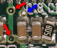
The tented vias look gold-plated to me, so unless the gold plating disappears, it doesn't look like the solder-mask-failure is going to cause any problems with copper oxidation.

I don't see how having a board with less solder or more arbitrarily aligned parts is going to perform any better. Just look at the IC's, they are spot-on, so it's just a pad-geometry problem with the small passive resistors and caps in that one tiny section. During manufacturing, the pick and place probably sets them perfectly on the pads and then they get skewed when they go through reflow.

I vote for "use the board, keep it." You may have some problems with the aesthetic of the board, but from a technical point of view there is no problem with how that's soldered.
 
Dec 2, 2009 at 3:25 AM Post #25 of 28
I finally figured out what was wrong with my PSU tester. it needed 'all' its connections plugged in, even the 4 wire pentium4 cpu plug and the 4pin drive molex. I didn't know it cared about that but that's why it was beeping and that's what '12v #2' meant, it was referring to the drive molex connector. I'll shoot pic of that PSU tester later.

but the pico-psu DOES seem to pass the power supply tester. I guess I'll try a real mobo next (not my actual intended one, though; I'm going to take baby steps on this pico thing)
wink.gif
 
Dec 2, 2009 at 7:39 AM Post #26 of 28
I'm sure it's fine, but I'd shoot them an email and mention they could probably improve on the fab. Chances are they aren't even looking at them much - some engineer designed it, shipped off the specs to China, they get them back in boxes and ship them out.

Also, kind of off topic, but what would the purpose be of tenting vias? Why not just leave them open and have them immersed in tin like a pad (how normal vias are done)?
 
Dec 2, 2009 at 8:52 AM Post #27 of 28
I believe one of the main reasons for the use of tented vias is to avoid breaking up labels and graphics on the silkscreen.

Also, with a tented via you would be less prone to accidental solder bridges when soldering components or shorting when probing the board I guess, although that would depend on the pcb layout in question.
 
Dec 2, 2009 at 11:45 AM Post #28 of 28
Tenting a via would seem to be an mostly an aesthetic thing. It came up in another thread and I went looking for info and it all seemed to be about look. However, with a via under a chip, it would help to ensure that there are no hidden bridges.

The problem I've read is that it is better done with dry-film mask as opposed to photoimagable. To do it with photoimagable, it seems you shoud either fill or plug the via first to proper finish on the soldermask.
 

Users who are viewing this thread

Back
Top