Millett Hybrid Diamond Buffer Construction Thread.
Feb 24, 2006 at 11:12 PM Thread Starter Post #1 of 17

headchange4u

500+ Head-Fier
Joined
Jan 3, 2005
Posts
739
Likes
11
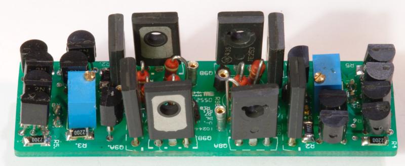
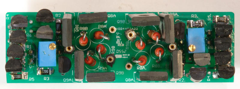
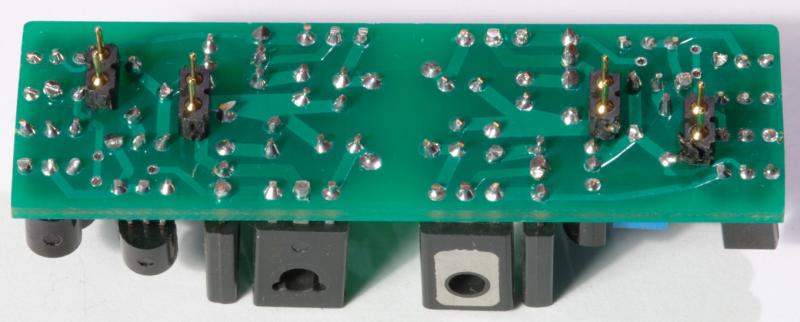
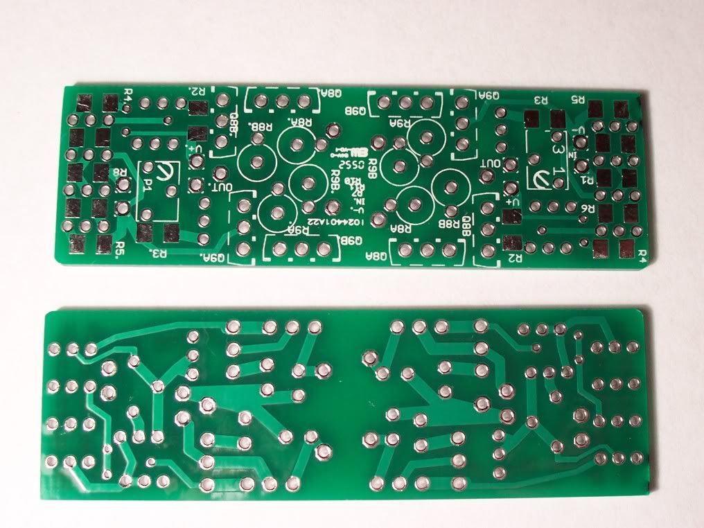
Reference pic of a Millet Hybrid Diamond Buffer (dDB) PCB:
MilletHybriddBf009.jpg


[size=medium]DIYforums.org Millet Hybrid Homepage[/size]
Group Buy Thread

dDB Contruction Overview (contains DIYforums.org and Headwize dDB related threads)
Desgn
Parts List
Assembly Instructions and Bias Adjustment
FAQ

I just got my dDB in from Nate today and I though I would start a construction thread for Head-Fi members. These buffers do have some SMD solder work that has to be performed, so it's probably not the best project if it's the first time you have picked up a soldering iron.

Maybe someone could post a pic of a populated dDB PCB for reference?

Big thanks to Nate for organizing the group buy and a big thanks to all of those involved in the design of the dDB and the Millet.
 
Feb 25, 2006 at 2:28 AM Post #3 of 17
Thanks for the pic Alex.

I notice you have the caps that are mounted near the dDB on very long leads. Is there a problem with the clearance of the caps in that area?

Anybody have a pic of the bottom of a populated PCB so I can see the pins for mounting?
 
Feb 25, 2006 at 3:06 AM Post #4 of 17
the caps have long leads because of space requirements with the Buffer. if you look closely at his board (or your own) you should see a white rectangle around the buffer area, if anything crosses that the buffer will not fit. had AK mounted the capacitors flush on the board they would have crossed over this line and he wouldnt have been able to insert the buffer.

on a side note, AK would you please post a close up of your SMD soldering.
icon10.gif


wow AK that was an incredible response time! thanks!
 
Feb 25, 2006 at 3:06 AM Post #5 of 17
Quote:

Originally Posted by headchange4u
Thanks for the pic Alex.

I notice you have the caps that are mounted near the dDB on very long leads. Is there a problem with the clearance of the caps in that area?

Anybody have a pic of the bottom of a populated PCB so I can see the pins for mounting?


I have way oversized caps there so yes they don't fit there.
 
Feb 25, 2006 at 3:07 AM Post #6 of 17
Quote:

Originally Posted by jerb
the caps have long leads because of space requirements with the Buffer. if you look closely at his board (or your own) you should see a white rectangle around the buffer area, if anything crosses that the buffer will not fit. had AK mounted the capacitors flush on the board they would have crossed over this line and he wouldnt have been able to insert the buffer.

on a side note, AK would you please post a close up of your SMD soldering.
icon10.gif


Yea I will get a pic once my friend comes over. My camera can't do macro mode.

-Alex-
 
Feb 28, 2006 at 2:17 AM Post #8 of 17
Quote:

Originally Posted by [AK]Zip
I have way oversized caps there so yes they don't fit there.


I wonder if taking a half-round file to the buffer board would allow the caps to sit flush again. It looks like at least 1mm or 2 could be removed. Are they 12.5mm caps on 10mm cap allowance?
 
Feb 28, 2006 at 2:21 AM Post #9 of 17
Quote:

Originally Posted by SHLim
Appreciate if someone can post a photo of the under side of the DB with the pin soldered.

Sam


I will get a picture for you here in a little bit.
smily_headphones1.gif


Quote:

Originally Posted by mono
I wonder if taking a half-round file to the buffer board would allow the caps to sit flush again. It looks like at least 1mm or 2 could be removed. Are they 12.5mm caps on 10mm cap allowance?


Whatever size the white circle is. That is the max cap size you can fit in there sitting strait up and down.

-Alex-
 

Users who are viewing this thread

Back
Top