12AU7 PCB Starving Student Hybrid Amp - zammykoo Build Log
Aug 30, 2011 at 12:35 AM Thread Starter Post #1 of 59

zammykoo

100+ Head-Fier
Joined
Jun 11, 2011
Posts
275
Likes
20
Hey all, this will be my 12AU7 SS build log. I wanted to separate my design thread from the actual build, but for reference you can find it here
 
Many thanks goes to Dsavitsk and TomB!
 
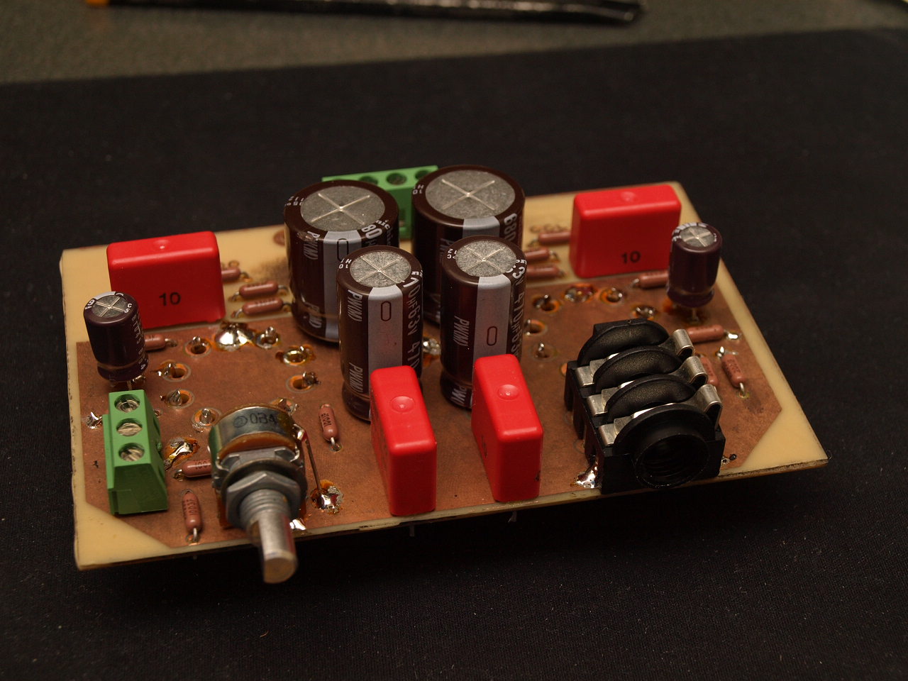
Etch today, drill tomorrorw:

 
Aug 30, 2011 at 9:56 PM Post #4 of 59
Thanks fellas,
 
The top side of this board looks good but the ground plane got a bit messy. I'm going to try and make a better pcb for the build. This is my first time making double sided copper boards, it's quite tough.
 
I did this with the good ol' toner transfer method
smily_headphones1.gif

 
Aug 31, 2011 at 12:35 AM Post #5 of 59
Hey! Can I use your PCB design too? I'm doing a project in school and I wanted to etch a board with CnC the drill it. I was about to post for something I could put into MasterCAM but it looks like I found it! Can you send me a PM or post up your design sheet so I can take it learn from it then etch a PCB for class?
 
Thanks!!!
 
Aug 31, 2011 at 8:55 AM Post #7 of 59
Try some of the advice here for your next etch and you might
get a better ground plane.
Otherwise, good job for a first try at a double sided board!
 
Aug 31, 2011 at 10:53 AM Post #8 of 59


Quote:
Try some of the advice here for your next etch and you might
get a better ground plane.
Otherwise, good job for a first try at a double sided board!


Funny that you mention this because I found that thread just last night! I'll definitely give that a try. But to be honest, I think I just didn't apply enough heat to the toner on the ground plane side. Since I've never had to transfer such a solid area before I didn't know how long to expect.
 
Sep 5, 2011 at 5:53 PM Post #9 of 59
Been super busy so I've only been able to do a bit at a time. Etched a couple more pcbs and got the ground plane down pretty good.
 
Question for PCB experts:
There is one issue that I didn't see ahead of time (because I'm new to etching double sided plates) that some components, like the capacitors, sit completely flat on the board where it does not allow any space beneath for the soldering iron tip to. For example if I need to solder the caps to the ground plane... how do i do that?


Sep 5, 2011 at 6:37 PM Post #10 of 59
EDIT: Ah ... I see what you're asking.  On the manufactured PCB, one of the leads of each capacitor is soldered to a pad that's connected to the ground plane, where the ground plane forms the negative connection to the entire amp.  Maybe what we're missing here is the fact that manufactured PCB's have through-plated holes and when you solder on the backside, that counts as soldering on the front side, too.
 
Looks like a nice job with the PCB's, by the way.  They almost look like one of the non-silk-screened prototypes that Dsavitsk ran.
wink.gif

 
EDIT: If you can't run additional traces on the top side, maybe you need some make-shift vias by soldering additional small holes that will allow a jumper connection through to the ground plane?  I don't know - maybe someone who's had some more experience etching their own has some better ideas.
 
Sep 5, 2011 at 6:50 PM Post #11 of 59
Tom, thanks for chiming in.
 
I think you've answered my question about the manufactured pcb holes being connected on both sides... and since my double sided board holes do not connect from front to back, I'll have to drill additional holes next to the cap ground holes and bend the leads up back through to the ground plane to be able to solder the points.
 
Any other suggestions for a quick solution?
 
Sep 5, 2011 at 8:27 PM Post #12 of 59


Quote:
Tom, thanks for chiming in.
 
I think you've answered my question about the manufactured pcb holes being connected on both sides... and since my double sided board holes do not connect from front to back, I'll have to drill additional holes next to the cap ground holes and bend the leads up back through to the ground plane to be able to solder the points.
 
Any other suggestions for a quick solution?


It's probably a kludge in either case, but quality electrolytics have a rubber pad on the bottom.  This would allow you to bend the ground lead out at a 90 degree angle, parallel to the ground plane, and solder it directly.  The electrolytic can still be flush to the PCB when you do this.  Look at one of the electrolytics with a rubber pad and you'll see what I mean.  Note that you may still have a bit of difficulty with this, because manufactured PCB's use "relieving" at the ground pads, where the metal is only connecting at four tiny points on the pad circle.  This gives a soldering iron the chance to heat up the pad locally without the ground plane "sinking" the heat throughout the entire PCB.


Sep 5, 2011 at 8:45 PM Post #13 of 59
Ah, I see what you mean. I took a look at the rubber pad and looks like there is an inset groove that I can kind of twist/turn the lead inside of. Is that what you mean?
 
I'll have to review the pcb again to determine if I have enough space to do either method... since I don't have all of my components yet.
 
Thanks
 
Sep 5, 2011 at 11:57 PM Post #14 of 59
Good job Tam. Looking good. Hopefully I'll have everything ready for you to test out.
 
Thanks for letting me use your design!
 
Ps. Arent you supposed to put enough solder to wick up to both planes?
 
http://www.diyforums.org/SSMH/construction/PCB-7.jpg
"When you look at the other side, inspect each pad for a "wicking" solder joint. The solder should travel all the way through to the other side and climb up slightly on the lead. If it doesn't, apply a slight bit of solder on the other side around the lead and the pad - just enough to make it look as if the wicking worked"
 
Sep 6, 2011 at 8:53 AM Post #15 of 59
When I do double sided boards, I plan ahead knowing there are no plate through holes.
If a component needs to be connected to a ground plane but covers up it's solder point,
I place a trace on the solderable side that is as short and thick as possible that leads
to a point where I can make a "via" to the ground plane. If there is enough clearance
under the component (or you don't mind it sticking up a bit), this point could be under
the component. You could also make the hole for the component a little bigger and just
solder an extra wire through the hole before hand to make a plate through hole.
 

Users who are viewing this thread

Back
Top