New DIY Altoids Tin Amp - The Pocket Class A "Wintergreen Handwarmer" by xrk971
May 14, 2017 at 4:57 PM Post #271 of 468
IMG_2094.JPG IMG_2095.JPG
Elna Silmic II
Nichicon KA, Muse KZ and Muse bipolar ES
Panasonic Oscon and FR
WIMA MKS, MKT, and SMD-PPS.
Vishay MKT and MKP
Kemet MMK and SMR
Tiny C0Gs from TDK and Kemet

So many combos to try...I've only had a little time to swap and listen but so far all I can say is dang, I can see why everybody loves Silmics!
 
May 17, 2017 at 11:46 AM Post #273 of 468

That's probably a good idea except I hate desoldering, and I'd have to remove the sockets later when I put the board back in it's tin. I've just been pushing the leads through the holes and getting surprisingly reliable contact.

So far I love the 35V 47uF Elna Silmic II on output bypass the best. It makes a noticeable improvement, whereas the small film bypasses are very hard to hear any difference with. The 25V 470uF Nichicon AK is already pretty clear-sounding. Even the 6.8uF WIMA is hard to hear. But the Silmic rocks the whole sound spectrum. More transparency, detail, smoothness, and even better bass. More on my impressions here:

http://www.diyaudio.com/forums/group-buys/302859-xrk971-pocket-class-headamp-gb-64.html#post5081205
 
Last edited:
May 17, 2017 at 4:02 PM Post #274 of 468
Hi @xrk971 ,

I just finished my first board and powered it up.

LED is lit, but no sound is coming through.

where should I start troubleshooting?

IMG_4727.JPG


IMG_4728.JPG


IMG_4729.JPG
 
Last edited:
May 17, 2017 at 4:58 PM Post #275 of 468
Hi @xrk971 ,

I just finished my first board and powered it up.

LED is lit, but no sound is coming through.

where should I start troubleshooting?

The obvious thing to check is probe the input connection and output connection for AC voltage. Maybe you simply have a bad joint in your connectors. Other than that, I would probe the pins of the MOSFET and post what your measurements are. gate voltage should be roughly 11.2V (via the spice sim on page 1) and the source should be at roughly 8.5V.

That's where I would start.

If those measure correctly, go probe the other labeled nodes in the spice simulation and let me know what doesn't line up. If they are all good we will just have to think a bit more.
 
Last edited:
May 17, 2017 at 5:14 PM Post #276 of 468
The obvious thing to check is probe the input connection and output connection for AC voltage. Maybe you simply have a bad joint in your connectors. Other than that, I would probe the pins of the MOSFET and post what your measurements are. gate voltage should be roughly 11.2V (via the spice sim on page 1) and the source should be at roughly 8.5V.

That's where I would start.

If those measure correctly, go probe the other labeled nodes in the spice simulation and let me know what doesn't line up. If they are all good we will just have to think a bit more.
thank you for the reply!

I measured mosfet and only got 2.95V and 3.11V for Pin 3 (the S pin from data sheet https://www.diodes.com/assets/Datasheets/ZVN4306G.pdf) and pins 1 and 2 are all 0v for both mosfets

I had trouble soldering the FETs, maybe poor connection or heat damage?
 
May 17, 2017 at 5:27 PM Post #277 of 468
thank you for the reply!

I measured mosfet and only got 2.95V and 3.11V for Pin 3 (the S pin from data sheet https://www.diodes.com/assets/Datasheets/ZVN4306G.pdf) and pins 1 and 2 are all 0v for both mosfets

I had trouble soldering the FETs, maybe poor connection or heat damage?

Could be. Does the JFET (the first one) have any good voltages? Might be easier if you use this as a reference.
9615488.png


Open the photo in paint or something and put your measured voltages in red at the appropriate locations. You could have broken the FETs but it's unlikely, in my opinion, that you wrecked the FETs on both sides. You don't get sound out of left or right, correct?
 
Last edited:
May 17, 2017 at 6:12 PM Post #278 of 468
Could be. Does the JFET (the first one) have any good voltages? Might be easier if you use this as a reference.
9615488.png


Open the photo in paint or something and put your measured voltages in red at the appropriate locations. You could have broken the FETs but it's unlikely, in my opinion, that you wrecked the FETs on both sides. You don't get sound out of left or right, correct?

both channels are silent.

I measured the following:
power = 18V
C1 = 18V (both caps)
C2 = 12V (both channels, both A and B caps)
C3 = 18V
C4 and C5 are all 18V
 
May 18, 2017 at 12:53 PM Post #280 of 468
DutchGFX,
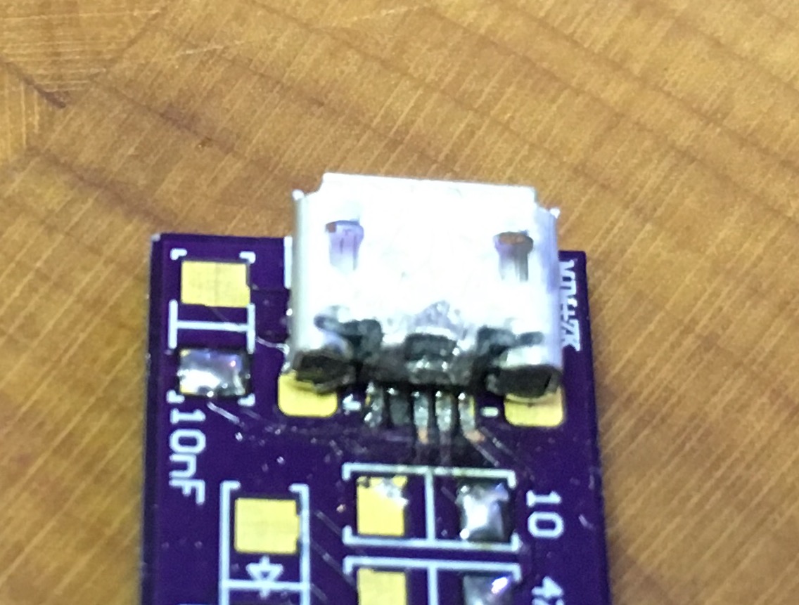
Thanks for stepping in to help! You are absolutely right. The first place to start is measure the 3 pins on the MOSFET. They pretty much tell the whole story.

Don't worry about clogging thread - this is where questions on how to debug should be posted.

Macky, (You are Babysupra on DIYA I guess)

On MOSFET just these 3 measures (relative to GND) will tell you if amp is working:

1. D (pin 2 or tab) says you have the main power applied to the amp (15 to 18v)
2. G (pin 1) says the gate voltage set by JFET is working (if off then check volts across R3) (7v to 9v)
3. S (pin 3) says bias current is flowing through resistor array and you have Class A action (6v to 8v)

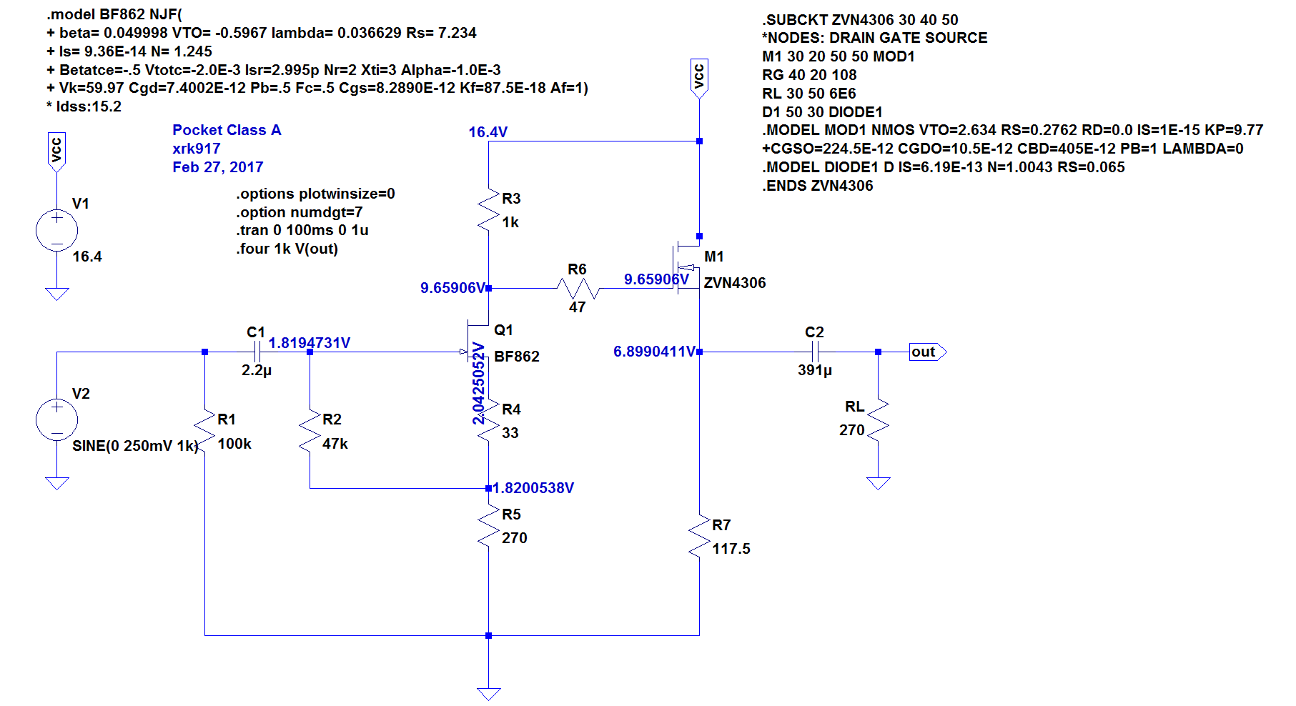
Here is what a nominal DC volts at all points should look like. It may be a little different for battery voltages and particualr JFET and MOSFETs, but not by much - maybe +/- 0.5 to 0.7v typically around the voltages in blue.

Here is schematic with a few more voltage test points:

616921d1495124663-xrk971-pocket-class-headamp-gb-pocket-class-schematic-v8-voltages.png


So the voltages around the JFET should be for DGS, circa 9.6v, 1.8v, 2.0v

For MOSFET DGS, circa 16,4v, 9,6v, 6.9v but in GDS pinout left to right 9.6v, 16.4v. 6.9v.

Across R3 is the voltage that tells you the bias across the JFET is 16.4-9.4v= 6.8v or 6.8mA across 1k

Across R7 is voltage that tells you the main MOSFET bias current 6.9v across 117.5R is 59mA

Voltage on inside (side facing JFET) should be 1.8v and corresponds to the DC bias setpoint on the gate of the JFET.

Install new MOSFETs and repeat measurement and report back - I suspect they are burned out with static zap.
 
Last edited:
May 18, 2017 at 2:12 PM Post #281 of 468
HI X and GDFX,

I took some DMM measurements relative to GND, and both right channel and left channel have same measurements:
C1 = C3 = C4 = C5 = JFET DGS = MOSFET DG = 14.8V
C2A = C2B = MOSFET S = 11.8V
R3 = 0V (using DMM 20V reading)

does this mean I have short circuit somewhere? (maybe even faulty fets?)

attached my pcb for reference.

IMG_4734.JPG
 
May 18, 2017 at 2:33 PM Post #282 of 468
R3 = 0V (using DMM 20V reading)

This confuses me. If you get 14.8V on the drain of the JFET, then how can R3 get 0V? It's as if you shorted R3 to ground, while managing to not connect it to the JFET drain, which surely isn't the issue here (I don't think).

Can you measure the voltage ACROSS R3? Put one probe on each end of R3.

At 0V from Drain to Source (they are both 14.8V) I reckon the JFET is in cutoff, so the voltage across R3 would be 0, so therefore both ends of R3 would be at roughly the power supply voltage. Since the MOSFET gate isn't shorted to the source (they are at different voltages) there is no path for current to flow through R3 to ground UNLESS it is flowing straight through the JFET, but the JFET source isn't even at ground, so I just don't see how R3 could be at ground.


I would remove the JFET. Then, since the MOSFET gate and source are both at PSU, it MUST be in saturation. By my calculation, if the JFET isn't present, and the PSU is 16.4V, then the SOURCE voltage on the MOSFET should be like 13.6V.

Remove the JFET, and measure the source voltage with respect to ground. That will tell us if the MOSFET is functioning properly
 
May 18, 2017 at 2:42 PM Post #283 of 468
This confuses me. If you get 14.8V on the drain of the JFET, then how can R3 get 0V? It's as if you shorted R3 to ground, while managing to not connect it to the JFET drain, which surely isn't the issue here (I don't think).

Can you measure the voltage ACROSS R3? Put one probe on each end of R3.

At 0V from Drain to Source (they are both 14.8V) I reckon the JFET is in cutoff, so the voltage across R3 would be 0, so therefore both ends of R3 would be at roughly the power supply voltage. Since the MOSFET gate isn't shorted to the source (they are at different voltages) there is no path for current to flow through R3 to ground UNLESS it is flowing straight through the JFET, but the JFET source isn't even at ground, so I just don't see how R3 could be at ground.


I would remove the JFET. Then, since the MOSFET gate and source are both at PSU, it MUST be in saturation. By my calculation, if the JFET isn't present, and the PSU is 16.4V, then the SOURCE voltage on the MOSFET should be like 13.6V.

Remove the JFET, and measure the source voltage with respect to ground. That will tell us if the MOSFET is functioning properly

sorry for the confusion!

so relative to GND, both ends of R3 reads 14.8V
directly probing both ends of R3 i get 0V

will remove JFETs reply back with measurement
 
May 18, 2017 at 2:43 PM Post #284 of 468
You measurements are still not clear to me. I would like the black probe of your DMM touching GND on the board (access on the GND pin (closest to edge of PCB) of the 3.5mm jack) and the red DMM probe looking at following on MOSFET: pin 1 (G), pin 2 (D), and pin 3 (S). I don't need to know anything about the voltage on the caps. Only the 3 pins of the MOSFET matter.

What is pin 1 (G) relative to GND? I assume same as pin 2 (D) = 14.8v?
Pin 3 (S) is 11.8v

Actually, I think you should remove the MOSFET and check to see if the JFET is functioning. The voltage at the drain of the JFET with the MOSFET missing should be the same as with it in place, if everything is working well.

Removing the JFET but leaving the MOSFET leaves no way for you to check if the MOSFET is good and no way to check if the JFET is good.

My guess is that that the MOSFET gate is shorted to the drain, and hence the gate leaks the 14.8v out to the bottom of R3 and thus voltage across R3 is zero. The MOSFET is basically running as if it is fully turned on with a 3.3v drop corresponding to Vgs for that MOSFET.

If you take out the MOSFET and the voltage across R3 is 6v to 7v, the JFET is good.

If the JFET went bad as in open-circuit, that could cause the MOSFET gate to be at same voltage as the drain with no current flowing through R3. But it is more likely that MOSFET gate blows before JFET gate blows.

Edit: I ran sim with R4 set to a high value to simulate an open circuit on JFET. It gives same values as your measurement. That the G and D pins of MOSFET same as PSU voltage 14.8v and S is 12v, and no voltage difference acriss R3. So in light of this, it sounds most likely that:

1. JFET is bad and failed in open circuit
2. cold solder joint on R4 or R5 or S pin of JFET

Try retouching solder points to eliminate cold solder joints around JFET or replace JFET.
 
Last edited:
May 18, 2017 at 3:08 PM Post #285 of 468
You measurements are still not clear to me. I would like the black probe of your DMM touching GND on the board (access on the GND pin (closest to edge of PCB) of the 3.5mm jack) and the red DMM probe looking at following on MOSFET: pin 1 (G), pin 2 (D), and pin 3 (S). I don't need to know anything about the voltage on the caps. Only the 3 pins of the MOSFET matter.

What is pin 1 (G) relative to GND? I assume same as pin 2 (D) = 14.8v?
Pin 3 (S) is 11.8v

Actually, I think you should remove the MOSFET and check to see if the JFET is functioning. The voltage at the drain of the JFET with the MOSFET missing should be the same as with it in place, if everything is working well.

Removing the JFET but leaving the MOSFET leaves no way for you to check if the MOSFET is good and no way to check if the JFET is good.

My guess is that that the MOSFET gate is shorted to the drain, and hence the gate leaks the 14.8v out to the bottom of R3 and thus voltage across R3 is zero. The MOSFET is basically running as if it is fully turned on with a 3.3v drop corresponding to Vgs for that MOSFET.

If you take out the MOSFET and the voltage across R3 is 6v to 7v, the JFET is good.

If the JFET went bad as in open-circuit, that could cause the MOSFET gate to be at same voltage as the drain with no current flowing through R3. But it is more likely that MOSFET gate blows before JFET gate blows.

Edit: I ran sim with R4 set to a high value to simulate an open circuit on JFET. It gives same values as your measurement. That the G and D pins of MOSFET same as PSU voltage 14.8v and S is 12v, and no voltage difference acriss R3. So in light of this, it sounds most likely that:

1. JFET is bad and failed in open circuit
2. cold solder joint on R4 or R5 or S pin of JFET

Try retouching solder points to eliminate cold solder joints around JFET or replace JFET.

black probe on the GND battery pin, and red probe on the DGS of Mosfet, i get following reading:
MOSFET Drain and Gate = 14.8V
MOSFET Source = 11.8V

black probe on the GND battery pin, and red probe on the DGS of JFET, i get following reading:
JFET Source, Drain and Gate = 14.8V

black and red probes on both sides of R3 i get 0V
 

Users who are viewing this thread

Back
Top