2 or 3 Channel, Single Ended Class "A" Design Thread
May 21, 2010 at 1:49 PM Thread Starter Post #1 of 87

Avro_Arrow

MOT: Soundwerx Designs
Joined
Apr 8, 2010
Posts
2,211
Likes
56
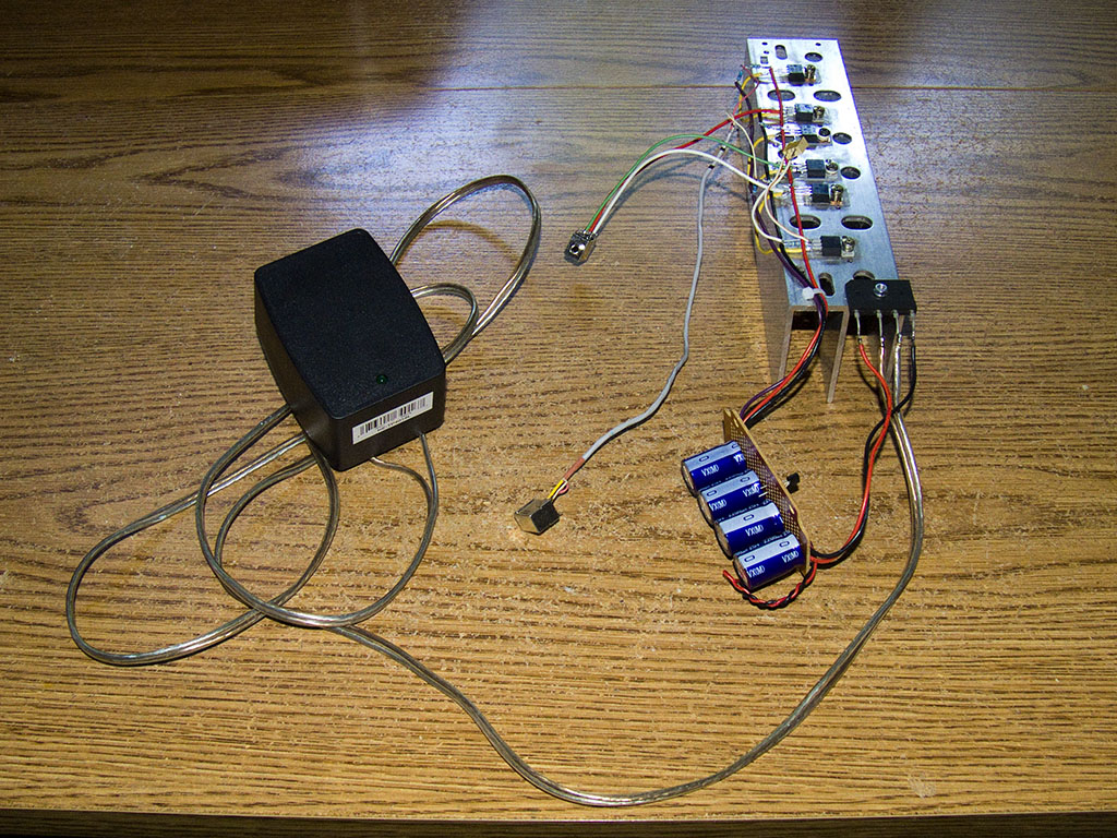
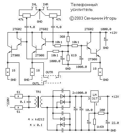
Here is my contribution to the DIY community.
You can use this on it's own as a Buffer or integrate
it into a larger design.
I'm open to improvements but wish to keep the design very simple.
The three channel layout has a high PSRR so you don't need
an elaborate power supply. I just use a simple full wave bridge
and caps. You can power from a center tap transformer or use
a TLE2426 to generate ground.


The trim pots let you zero out any DC offset but you should still try
and match components as close as you can.
 
May 21, 2010 at 3:35 PM Post #2 of 87
Lm317 is not good for sound - try use the second mosfet as CCS. Try this one, as for me, it's a best SE headphone buffer.  
It also work with mje3055, 2sc5200 and bd139 transistors.
 
May 21, 2010 at 4:37 PM Post #3 of 87
In the schematic you are using a simple resistor as your current sink. That
is fine to do but less efficient and not  necessarily better sound than LM317
current source/sink. I can see you have it tuned for low impedance headphones.
I have seen this done with MOSFET current sink and I may post a version
of that too if people want to try it. Also, with such a high PSRR you don't
really need a regulated power supply but it doesn't hurt either.
 
Quote:
Lm317 is not good for sound - try use the second mosfet as CCS. Try this one, as for me, it's a best SE headphone buffer.  
It also work with mje3055, 2sc5200 and bd139 transistors.


May 21, 2010 at 4:50 PM Post #5 of 87

I will try, but I would rather, like Ant1Xr1st did, people submit some of their ideas too...
What you are looking for in a good current source/sink is low noise and flat response.
Ring of two transistors are OK, LED biased transistor better, FET cascode, LED biased
transistor even better and FET/FET best. I know there are more but I'm not trying to be an
encyclopedia.
 
Quote:
I want to try different current sources. Can you show a current source with BD139 or BD140 and resistor?


May 21, 2010 at 6:33 PM Post #7 of 87
 
Quote:
I can see you have it tuned for low impedance headphones.

No. The bias is tuned for maximum transistor's linearity.
 
Quote:
with such a high PSRR you don't really need a regulated power supply but it doesn't hurt either

Such psu will be ok, but you will need C-R(or L)-C filter anyway. you may use a 7812 - it doesn't needed any extra resistors.
 
Quote:
simulate this frequency response

The simulation will not be correct because of simplified lm317 model.
 
Here is one more intresting schematic.

 
May 21, 2010 at 8:03 PM Post #8 of 87
Avro_Arrow, I have always liked the look of the 'active ground' (or whatever you call it) circuit since I first saw the scheme on the RJM site. However, as the Gate of the FET is ground referenced the Source must be at some negative voltage (about -1 to -3 Volts I guess, depending upon standing current). What then happens if the channel output is accidentally shorted to real (0 Volt) ground? Can the FET withstand the short, or will it pop?
 
Ant1Xr1st, thank you for showing these circuits. Regarding the last schematic, can the BSP129 be replaced by a FET with a lower internal impedance, to lower the output impedance? (Which type ?)
 
 
(I hope other people join in, because this can become an interesting thread...)
 
May 21, 2010 at 8:47 PM Post #9 of 87
The source sits at Vgs below ground (or virtual ground). In my example, Vgs was 3.65.
Right now I am using a 24 volt unregulated supply.
My outputs sit about 8 volts above V-.
Current through the device is limited by the current source to (in my case) 152.2 mA.
I don't think a short to either V+ or V- would cause it to pop. That is not to say that there
is no way to pop it, it just might take some "creative shorting".
Maybe I will try it with one of my "less well" matched IRF510s.
My IRFs are match to .01 volts.
They are all mounted on the same heat sink as well to combat thermal drift.
There is a picture of this amp in my Album or in the "pictures of your builds" thread.
 
Quote:
Avro_Arrow, I have always liked the look of the 'active ground' (or whatever you call it) circuit since I first saw the scheme on the RJM site. However, as the Gate of the FET is ground referenced the Source must be at some negative voltage (about -1 to -3 Volts I guess, depending upon standing current). What then happens if the channel output is accidentally shorted to real (0 Volt) ground? Can the FET withstand the short, or will it pop?
 
Ant1Xr1st, thank you for showing these circuits. Regarding the last schematic, can the BSP129 be replaced by a FET with a lower internal impedance, to lower the output impedance? (Which type ?)
 
 
(I hope other people join in, because this can become an interesting thread...)


May 21, 2010 at 8:50 PM Post #10 of 87
The fet is ccs'd. It shouldn't pop.
There is no good replacement for bsp129.
http://translate.google.com/translate?js=y&prev=_t&hl=ru&ie=UTF-8&layout=1&eotf=1&u=http%3A%2F%2Fmusatoffcv.narod.ru%2FProjects%2FHA-1.htm&sl=ru&tl=en
 
May 21, 2010 at 9:06 PM Post #12 of 87
Your LED bias is not done right.
LED goes to ground through a limiting resistor,
not directly to ground.
 
on second thought..it just all wrong...sorry

 
Quote:
I don't know if this works: 


Users who are viewing this thread

Back
Top