Virtual Ground (regulated!) - and Rail Splitter Circuits!
Mar 13, 2013 at 10:44 PM Post #76 of 125
Quote:
I think it works in the sim though, as each transistor is turning on enough to push the output into the middle.

 
No it's not. It's fubar.
 
Split the voltage source into 2, connect the midpoint to ground (like in my sim) and try again. If you connect the output to ground like you did, the simulator just forces it to 0V and you get a nonsense result...


w
 
Mar 13, 2013 at 11:09 PM Post #77 of 125
Quote:
 
No it's not. It's fubar

frown.gif


Split the voltage source into 2, connect the midpoint to ground (like in my sim) and try again. If you connect the output to ground like you did, the simulator just forces it to 0V and you get a nonsense result...

That may explain a few anomalies i got with the sim lol.
Back to the drawing board.
deadhorse.gif


Thanks w. I've been learning so much from your posts recently - Wakipedia.
 
Mar 15, 2013 at 1:04 AM Post #79 of 125
Quote:
Hello KT88,
 
Good idea - the voltage reference. Um, I am not "against" that at all. Draw your preferred schematic for that and post it, please? However, it appears that this circuit, with or without a trimmer pot, works well for my application. The voltage regulators hold the ground point at one potential better, it seems, better than other circuits which "drive" the ground point with discreet transistors with or without opamps - my guess as to why the original posted circuit sounds so good too...
 

 ​

Hello goldpoint,
 
sorry for the very late response, didn't really have time to open my laptop until now.
The idea is exactly what I've posted earlier with the zener, but instead it can be replaced with a reference IC (the exact model still has to be determined, there are many options, both 2 and 3 terminals).
 
So the LM317/337 and everything after that is the same as in your schematic, but the voltage divider with the diodes is replaced with this structure:

and the zener is actually a voltage reference IC. We must use a reference voltage of about 2.6V so it'll allow trimming for worst possible variations of the LM317/337. As I've stated before, the use of the resistive divider in parallel with the reference also allows the use of a relatively small capacitor for filtering in parallel with the trimmer (since the incremental resistance of the zener/diodes/reference is very small and would require large caps in parallel with it). This will help lower the noise significantly.
 
Edit: when I think about it a little more, the circuit can actually be simplified further. Since we can live with a small error between the 2 supply's, we can use a reference of 3V and than use just the trimmer in parallel without any resistors in series with it:

Now there are 2 resistors less which makes the circuit even nicer, and it still allows trimming for every possible value of the internal reference of the regulators. There could be an error between the supplies, which we should be able to live with (up to ~500mV between the 2 supplies). There is one other drawback with this circuit compared to the one with the 2 extra resistors, and that's the resolution of the adjustment the trimmer allows which is now not as good since any change in the trimmer directly translates to a similar part of the reference voltage. With a 10-turn trimmer this shouldn't be a problem.
 
There's also the option to use an IC that lets you choose between 2.5V or 3V (the AD780 is the first option I though of, but its very expensive so we won't use it, I guess there are others as well), so as long as the reference of the regulators combined is 2.5V or below (50% of times or maybe even more) you set the reference IC to 2.5V and only get a few mV's of imbalance, and if the regulators references combined are above 2.5V you set the reference IC to 3V and than you have to pay a little extra in the imbalance. The problem using the 2.5V state is the it'll be very close to the reference of the regulators, so the trimmer will be set very close to the limit. This means there's very little resistance between the reference IC (which has low incremental resistance) and the output of the trimmer, and therefore if we'd like to add a filtering cap in parallel to the output of the trimmer we'll have to use a large cap.
 
 
Mar 15, 2013 at 2:38 AM Post #80 of 125
KT88,
 
Thank you again. Do you like the TL431 series from ST Microelectronics?  see:  http://www.st.com/web/catalog/sense_power/FM1963/SC1771/SS1408/PF65361?s_searchtype=partnumber
Could I burden you to draw the exact schematic you are describing? (Or at least the voltage divider section. My power supplies are either 15V or 18V.) Include the recommended resistor and capacitor values...
 
Mar 15, 2013 at 12:14 PM Post #81 of 125
I want to start off by apologizing for the very long post :)
 
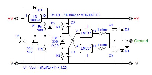
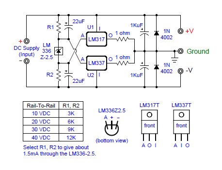
I'm not sure if the TL431 is the best options, its tempco isn't as low as some of the other IC's available in the market. However, the schematic will be similar with all of these. Here's a something basic:

 
R=(Vsupply_min-2.7)/0.003 - this will allow at least 1.5mA (a little less because of the resistors in parallel) of current through the reference at all times, which ensures it doesn't stop working correctly.
The reference is of a different model, but I've only used it for its symbol, the TL431 could be used instead.
The 1K-10K will ensure the output voltage is >2.684+2u*1K=2.686V which is larger than the worst case reference of the regulators. The trimmer should be of a large value (5K or more) so it doesn't eat too much of the current in this branch of the circuit.
For an fc of 20Hz the cap should be about 22uF - but its optional.
With worst case variations in temperature (assuming we work with a temperature range of about 10-50C in the case of the amplifier) the reference will change by about +-10mV. There are other factors such as the tempco of Iref, the tempco if Iadj (of the regulators), and the tempco of the internal reference of the regulators (which only shows nominal curves in the datasheet). The variations due to current tempco are quite small in this case, so the references are the main issue here. assuming the reference of the regulators has an opposite tempco (which is possible due to variations) we can get as much as 10mA of extra current in the output 1R resistors. The even bigger problem is what will happen if the tempco's are opposite so that the reference IC goes higher and the regulators go lower, which will make the circuit stop working unless sufficient DC current was set with the trimmer.
 
However, this is indeed a worst case scenario. For 99.9% of times the zero tempco temperature of the reference will actually be in the vicinity of 25C so we should only see a change of 1-2mA at the output with a change of temperature of +-20C. I still think it would be better to replace the regulators for something with a lower minimum load current just to save power, but since that is very easy to do when building the circuit, its of less importance at the moment.
 
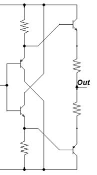
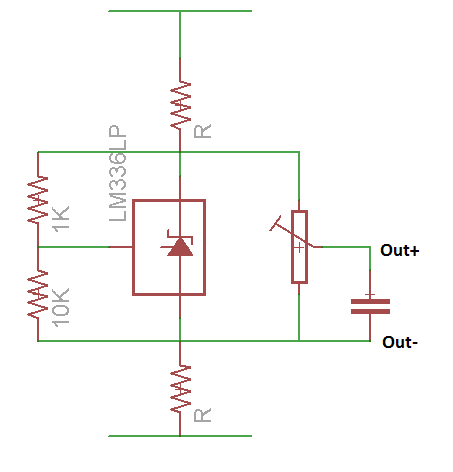
BTW, it is possible to change the circuit so it'll have less resistors and will look like this:

 
I would advice against this option for our use as it can't generate a reference voltage lower than the IC's internal reference (which could be as high as 2.55V, depending on the exact model of the IC).
 
Its also possible to implement the voltage divider using a fixed resistor and a trimmer in series. This option is also not as good as it both requires more parts, and uses a divider with parts of different tempco (a constant resistors and the trimmer).
 
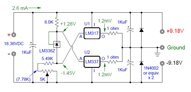
I have another question about this circuit. What happens if the amplifier it drives has a different DC current from each of the supplies? At DC the output caps do nothing, so if there's a constant DC current to/from the virtual GND the circuit might not work. Let assume you have a difference of 10mV's between the 317 and the 337 so a current of 5mA in the 1ohm resistors. Now we add some current (lets say 10mA) from the amplifier to the virtual GND (because there's a DC offset at the amplifiers output, or because someone used a LED returned to the virtual GND, or whatever). Now these 10mA go to the 337 through a 1ohm resistor, dropping 10mV across it. So now the 1ohm resistor at the output of the 317 has 0V across is, so no current is coming out of the 317, and its not operating as it should. This is a big issue with these output resistors since they make the output resistance of this structure very high at low frequencies.
 
A different direction:
The way we are trying to do this stabilization is actually not the smartest. If you'll think about it, we are trying to regulate the current using an open loop. By open loop I mean we have no feedback of what the actual current flowing through the resistors is. The best option to do this would be by setting the voltage of one regulator at ~Vin/2 using a simpler method such as resistive divider, and than regulating the adjustment pin of the second regulator to to keep a constant DC current at the output. This must only work on frequencies below the audio range.
 
If we try and solve both these issues (DC current causing the circuit to stop working, and keeping the current from rising significantly with changes in temperature) we should make some changes. This is the first idea I have of how to do this (its more complex than the circuit we were discussing, and I'm sure there are issues with it, but its an idea :)):

 
Keep in mind I didn't test/simulate this, this is just an idea. There's always the chance I've made some stupid mistake and the entire circuit won't work. Also don't pay attention to the part numbers, I just took some parts with the right symbols and didn't pay attention to the exact part number.
The idea of the circuit is quite simple actually:
R1-D1-R5 is a simple divider to create Vsupply/2-1.25V. This is used as the Adj voltage of the 337 to make the output Vin/2. D1 is a 2.5V zener (or 4 diodes), its exact voltage isn't very important, it'll just shift the virtual-GND around the mid-point a bit, it won't affect the current at the output.
Then the 317 is connected with its output directly to this point - but now there's a closed loop used to keep its DC current constant.
R2 is used as a current-shunt to create a voltage proportional to the current of the 317 regulator
R3-C1 is used as a LPF to make sure we only regulate the DC current (very slow changes like that of temperature), and don't affect AC dynamic of the circuit.
Q1-trimmer are used to generate a DC voltage referenced to the positive supply. The jfet is used as a CCS, the trimmer allows setting the DC voltage to the input of the op-amp.
The op-amp should be able to work with its inputs very close to the positive supply (perhaps something similar to the tl072 which is very cheap).
C2-R4 are used for compensation. The low frequency path is through IC4-R2-LPF, and so for stability we must allow a different feedback path at higher frequencies which is accomplished using C2. R4 is there to add a significant resistance between C2 and the supply in case the trimmer is of low resistance, or the amplifier will see a very low impedance load at high frequencies. It has to go the the inverting input while the low frequency feedback goes to the non-inverting because of the phase inversion from the regulator+R2 path (higher voltage at the output of the op-amp generates lower voltage at input of the op-amp).
The resistors R6-R7 can be much smaller now (in theory even omitted altogether), as we directly regulate the DC current of the 317, and the 337 will simply sink any current from the 317+the load.
To solve the issue of DC current from the amplifier all that has to be done is set the trimmer value accordingly. If the current is coming from the amplifier into the circuit, than just set a few mA in the 317, and the 337 will sink the current of the 317+the current coming from the amplifier. If current is flowing from the circuit to the amplifier the trimmer must be set so that the 317 has a few mA more than the current the amplifier draws, this will ensure the 337 is on and sinking current (or to sum it up, set the trimmer so both regulators have at least a couple of mA flowing in them).
 
The feedback factor B of the closed loop must be considered for stability. Assuming the regulator has a constant voltage between the adjust and the out pins (gain of ~1) we get:
B=1*R2/[(R6+R7)*(1+sC1R3)] at lower frequencies. This means we might indeed have an issue with stability unless we use a very low frequency at the LPF (the lower R6+R7, the lower the BW must be). C2 helps us with stability since B=~1 at higher frequencies, maintaining sufficient phase margin.
The current value is set by the trimmer, and it'll be (Vtrimmer/R2=Ijfet*Rtrimmer/R2) where Vtrimmer is the voltage between the two pins of the trimmer. The exact value of the jfet current isn't critical since we can set the trimmer to compensate for that.
 
I want to repeat it once more, this is just an idea I've had, and I've only made a very quick stability analysis which at least to me seems to make sense. If anyone could go over it and verify it'll be great, a fresh point of view is always welcome. If anyone would like to prototype it/simulate it, I'll be more than happy to help with calculation of the components values.
 
I apologize once more for the long post :)
 
Edit:
there's a mistake in the schematic, the Adj of the 337 should connect above the zener and not below it.
 
Mar 15, 2013 at 4:48 PM Post #82 of 125
I see you are a member of the trade goldpoint. Why haven't you registered the fact with Head-Fi moderators?
 
http://www.goldpt.com/index.html
 
No Members of the Trade can use his/her business name, product name, brand name, postal address, e-mail address, telephone number or URL as part of his/her Head-Fi username. All Members of the Trade must contact the forum administrator at jude@head-fi.org to notify him of an interest in posting before making any posts. If a forum member who was not previously a Member of the Trade becomes a Member of the Trade, he must notify the forum administrator of the change in status. After notification of the "Member of the Trade" status, the forum administrator will then add the appropriate tag (Audio Dealer, Manufacturer, Distributor, etc.) to the appropriate profile(s).
 
w
 
Mar 15, 2013 at 6:42 PM Post #84 of 125
Oops! At least I can see who blew the whistle! Obviously, we should read the Service Agreements BEFORE we post! Thank you for your continual help WakiBaki. I guess that you will be seeing me as a different name soon. I am hoping all your simulations work out well. Sincerely, the guy.
 
 
Mar 15, 2013 at 7:47 PM Post #85 of 125
Goldpoint KT88, there's a major flaw in your latest design : R2 is in the path of V+.
 
So that any current flowing out through V+ and being sunk back trough the LM337 is also affecting the voltage across R2.
 
I doubt that's an efficient way of using an op-amp anyways. And honestly, the moment you introduce an op-amp in the circuit is the moment the regulators become redundant. There is no reason not to use a simple circuit like wakibaki posted on page 4. And it's just so, so, so much prettier. And guess what? His design has a significantly lower part counts. Does this not make his design easier and cheaper to build?
 
edit: the post was so long I forgot who wrote it. 
 
Mar 15, 2013 at 8:15 PM Post #86 of 125
Hi Kim,
 
Um, that's not MY design, it's KT88's design you know.  But I like MY design because the voltage regulators HOLD the ground point in place, (either the iteration with two adjustable regulators or the original posting iteration with two fixed regulators and a pre-regulator). Even though the zener approach did not work out, I hope to implement KT88's possible voltage reference approach.
 
Mar 15, 2013 at 11:30 PM Post #87 of 125
Quote:
To solve the issue of DC current from the amplifier all that has to be done is set the trimmer value accordingly

 
Ignoring for the moment the fact that your circuit doesn't work, KT88, anything with a trimmer is just nonsense. Something that needs trimmed to accomodate the amplifier is double nonsense.
 
We're looking for self adjusting.
 

Hello KT88,
 
<>  What we're trying to do is create a simple, inexpensive "self adjusting" virtual ground which has very low quiescent current - for use with batteries.
 
<>  Self adjusting - so that a wide range of battery voltages could be used with it.
 
<>  The virtual ground can be perhaps 0.1V or so above or below the exact "1/2 rail-to-rail voltage".
 
<>  It seems using the readily available, inexpensive LM317/337 complimentary regulators is one good place to start from - high precision is not a goal on this...


Originally Posted by goldpoint /img/forum/go_quote.gif
 
I like MY design because the voltage regulators HOLD the ground point in place


Yeah, that's what you say, but anybody who reads the whole of the thread will know that if you're building an amplifier, the circuit you'll use will be mine, because it will SOUND BETTER, COST LESS and have BETTER BATTERY LIFE.
 
w
 
Mar 16, 2013 at 1:00 AM Post #88 of 125
Quote:
Goldpoint KT88, there's a major flaw in your latest design : R2 is in the path of V+.


Of course R2 is in the way, its used as a current shunt :)
It can be in the order of a few ohms which is low enough to have no effect for something like a headphone amplifier.
 
 
Quote:
I doubt that's an efficient way of using an op-amp anyways. And honestly, the moment you introduce an op-amp in the circuit is the moment the regulators become redundant. There is no reason not to use a simple circuit like wakibaki posted on page 4. And it's just so, so, so much prettier. And guess what? His design has a significantly lower part counts. Does this not make his design easier and cheaper to build?
 

A. That's what I've said earlier in this thread, there are other simpler ways that do it well. The entire thread as far as I see it is mainly having some fun, to see what other not-standard ways to do this we can come up with.
B. Yes, the 317 here is just used as a follower, a transistor will do the exact same job in this case.
C. In the same circuit you've linked to, I think it will be even better to have a single op-amp instead of two, and have the feedback coming from the output instead of the emitters (obviously it would be best to add a couple of diodes between the bases of the transistors to bias it in a class-AB form). This will include the resistors within the loop and will drop the output resistance even lower. This will be similar to using an op-amp with large current sourcing/sinking capability as a follower or a simple buffer IC, which is basically the easiest way to accomplish that.
D. The circuit wakibaki posted, as it is right now, also has an issue with a constant DC current at the output. Lets say we have 10mA from the vGND to the negative supply. This means that the vGND voltage is 0-10m*R3=-1mV. So now the voltage across R4 is -1mV and current should flow from Q2 to R4. But it can't be done since its a PNP and it can only sink current, so now U2 will see 1mV across its inputs and will saturate the output of the op-amp to the positive supply. This will lead to a turn-on delay when Q2 will have to sink AC current from the load since the op-amp will have to slew half of the entire supply voltage to turn Q2 on. In fact, there's a much more serious problem. If the supply voltage is high enough (>10V), the VBE voltage will be higher than the maximum allowable voltage of the transistor and it'll fry, so this circuit has a very serious problem. It might even happen without any load at the output, just replace the polarities of the offset voltages of the 2 op-amps (so the voltage at Q2 will try and be a little higher than at Q1 - which can't be done because of the transistor polarities), and the offset might be high enough to fry both transistors. So the circuit as it is actually doesn't work at all.
 
Quote:
 
Ignoring for the moment the fact that your circuit doesn't work, KT88, anything with a trimmer is just nonsense. Something that needs trimmed to accomodate the amplifier is double nonsense.
 
We're looking for self adjusting.
 
 
w

 
Lets not ignore the fact it doesn't work. While I don't really mind since I'm not going to build it, I would like to see what I've missed that will make it not work.
 
BTW, I've made a small mistake in the schematic, obviously the regulator should actually connect with its Adj above the zener and not below it or the voltage will not be ~Vin/2. The lower regulator is the 337, and the one in the feedback loop is the 317 in case it wasn't clear.
 
Mar 16, 2013 at 1:45 AM Post #89 of 125
Here's a different and simplified approach at the same thing:


The zener is a 2.5V as before, and it is used to set the adjust pin on the 337 (only this time I didn't make the same mistake, and the connection is above the zener so Vout=Vin/2).
R9 has a DC voltage of 1.25V across it which is used to set the current the 317 at DC (for 10mA it should be ~120ohms).
C3 is there for bypass at higher frequencies - 220uF should give a cut-off frequency of about 5Hz in this case (with a 120R resistor for R9). A low -ESR cap should be used here.
 
The thermal stability issue of the DC current is solved since the 317 has feedback of this current using R9. This circuit doesn't solve the issue of having a constant DC current flowing out of the vGND into the load unless this current is lower than the current in R9 (it does handle the opposite case where the current is coming from the load into the circuit), so that issue still has to be solved somehow.
 
Mar 16, 2013 at 3:08 AM Post #90 of 125
Wow, fully untrue Wakibaki. I prefer my own tried and tested circuit - for reasons already stated repeatedly.
 
This whole virtual ground thread I started sure took off like wildfire, eh? Don't you also "just hate" my original post which started the thread? To each his own, child.
 

Users who are viewing this thread

Back
Top