rectifier bridge basics
Mar 14, 2003 at 10:50 AM Thread Starter Post #1 of 34

ofb

100+ Head-Fier
Joined
Sep 22, 2002
Posts
124
Likes
10
okay, this is a classic case of the eraser wearing out before the pencil, so i'd best ask for help. i'm looking at the circuit diagram for the SDS psu and its pcb.

http://headwize2.powerpill.org/proje...stokes_prj.htm

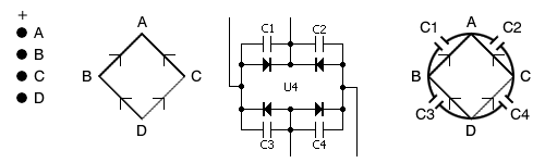
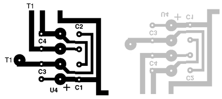
i'm trying to understand how the circuit relates to the legs of the rectifier bridge. it seems clear to me that the inner legs are for the ac, and the outer two are the dc. but look at c1 and c2 on the pcb. ... shouldn't they be linking an outer leg and an inner leg each? is the pcb not showing c2 links the inner legs and c1 the outer legs?

what am i screwing up here?
 
Mar 14, 2003 at 3:23 PM Post #2 of 34
The way I interpret this is that the outer connection points are the AC (to tranny) and the inner (center) pair are going to the rails (DC). Imagine grabbing the upper and lower center points, and stretching them outwards vertically, so that the shape resembles a diamond. Now it's a one-piece full-wave bridge, with AC on the "east and west" corners, and DC from the "north and sounth" corners. The caps just bypass each diode in the bridge.

Make sense?
 
Mar 14, 2003 at 7:41 PM Post #3 of 34
Quote:

Originally posted by Voodoochile
Make sense?


well, no, actually.
smily_headphones1.gif


let's got through this step by step and perhaps you can tell me where my thinking is confused.

first off, the bridge spec'd in the sds actually has pins marked + ~ - . so for this one the center two are the AC from the tranny, and the outer pins are the pos and neg. right?

now let's do what you said and redraw it as a diamond.

bridge_sketch1.gif


the first sketch is the component pins lettered. the second is the schematic for that component. the third is the psu circuit for the SDS. the forth is my second sketch again with "The caps just bypass each diode in the bridge", as you say.

now look at the pcb for the SDS psu. left is originial, which is a bottom view of course, and right is the same thing flipped if that's any help in clarity.

bridge_sketch2.gif


see the two legs of C2 connect to the two inner legs of the rectifier? and the two legs of C1 connect to the two outer legs of the rectifer...

to repeat what i said to myself last night at this point, "huh-what?"

shouldn't that be C1 and C2 each connect an outer leg and the farther inner leg each, in order to match the first sketches?
 
Mar 14, 2003 at 7:47 PM Post #4 of 34
Everything in the first graphic is true... A = +, D = -, B&C=AC in. That's all good.

As for the copper patter, I've never really looked closely at it, but I do know that others have etched it and it works as planned.

I'm checking it out now.
smily_headphones1.gif


It appears that C2 and C3's labels are swapped on the copper???
Interesting find, I never noticed, probably because I have never made this PCB. It appears that it would work fine as is, but that the labelling is wrong.

I have made the same circuit w/o the amp, but using seperate diodes VS the inline bridge.

EDIT: I take that back, is the pinout correct for the bridge??? It does look as though there is a cap between tha AC rails?
 
Mar 14, 2003 at 8:11 PM Post #5 of 34
Quote:

Originally posted by Voodoochile
I have made the same circuit w/o the amp, but using seperate diodes VS the inline bridge.


yeah, as did erix with Son o' ****. i was following suit but using the bridge spec'd in the SDS article and then found the apparent glitch. naturally i'm confused.

Quote:

It appears that C2 and C3's labels are swapped on the copper???


well, no. the caps are all the same so the numbering is incidental. the circuit still appears wrong. caps would have to connect AB CD AC BD. hrm.

really weird because it's not like that pcb is new.
 
Mar 14, 2003 at 8:15 PM Post #6 of 34
Yes, per my edit... there is something awry here.
As it's labelled, C2 does indeed bypass from AC-to-AC. I have no idea what that is supposed to imply though. Id does not appear to match the schematic at all.

Now I'm confused.

In your initial post, I thought you were having trouble making sense of the schematic diagramming, which would lead you to believe that it is discrete diode design, but the foil is drawn for the inline bridge, and looks totally different from the schematic.
 
Mar 14, 2003 at 8:25 PM Post #7 of 34
Quote:

Originally posted by Voodoochile
EDIT: I take that back, is the pinout correct for the bridge??? It does look as though there is a cap between tha AC rails?


well, the component has impressed on the top "+ ~ -". it has silkscreend on the side "+ AC -".

and here's the datasheet pdf:http://rocky.digikey.com/WebLib/Diod...01l-rs407l.pdf

looks like the inner two are the AC to me. look like that to you?
 
Mar 14, 2003 at 8:28 PM Post #8 of 34
Yes, plus I followed the traces from the transformer pins to the bridge. The two inner pins are absolutely AC in.
 
Mar 14, 2003 at 8:56 PM Post #9 of 34
well, golly.

being my first project, i'm not having the warm fuzzies about this.

you don't suppose that pcb is incorrect but actually works? hence no one has mentioned it? i'm grasping at straws of understanding here.

this also leads to what i meant to ask later on: what's the idea of the bypass caps c1 through c4 anyway? most diode bridges i see don't have those. i may not be able to understand the explanation yet, but i'd like to try.
 
Mar 14, 2003 at 9:05 PM Post #10 of 34
Short answer: the diode bypass caps help to smooth out the DC from the bridge.

The board may or may not be fine as is, but it surely does not match the schematic offered along with it. Try emailing Sheldon, perhaps.
 
Mar 14, 2003 at 9:35 PM Post #11 of 34
The board looks wrong to me, it puts a bypass cap across the AC line, the schematic does not do that.

The schematic is known to work, I have built from it myself. I'm not sure what would happen using the board as shown.
 
Mar 14, 2003 at 11:41 PM Post #12 of 34
i've written sheldon. perhaps he'll get a moment to look into it.

since i've got the bridge i'll use that, although one can't hitch it up in this circuit without crossing a leg somewhere.

just curious: if one were to do this with individual diodes, you could use the same as specified later in the circuit? it's a 1amp 1000v 1N4007GICT-ND. that's serious overkill, right?

and while i'm asking, are there any pros and cons to using a bridge vs four diodes in a psu like this?
 
Mar 15, 2003 at 1:21 AM Post #13 of 34
It would be fine to use 1N4007's everywhere. An advantage to doing so is that they are cheap. The 1N4007GICT-ND cost $0.04 each from Digikey, a KBL04 diode bridge is $2.07.
 
Mar 15, 2003 at 1:38 AM Post #14 of 34
I went to Sheldon's site to see if he had the amp on it, and it's not there. Interesting to see what he says.

I like individual diodes anyway- they are easier to bypass with caps (physically) and you can use better quality diodes, such as schottky's.
 
Mar 15, 2003 at 1:44 AM Post #15 of 34
A related question is if it is worthwhile to use exotic diodes like Schottky or ultrafast in audio applications. I tend to think that there would be little audible difference as long as the PS was well filtered and regulated, but I haven't tested this. I do note that Kevin Gilmore didn't specify exotic diodes in the design of the Class A headphone amp PSU.
 

Users who are viewing this thread

Back
Top