Post pics of your builds....
Jan 24, 2013 at 5:21 PM Post #8,896 of 9,811
Quote:
Wow! This has got to be one of the most cramped PCBs I've ever seen!
Very nice!
 
Is is just me or does the PCB look completely different from the outline?

 
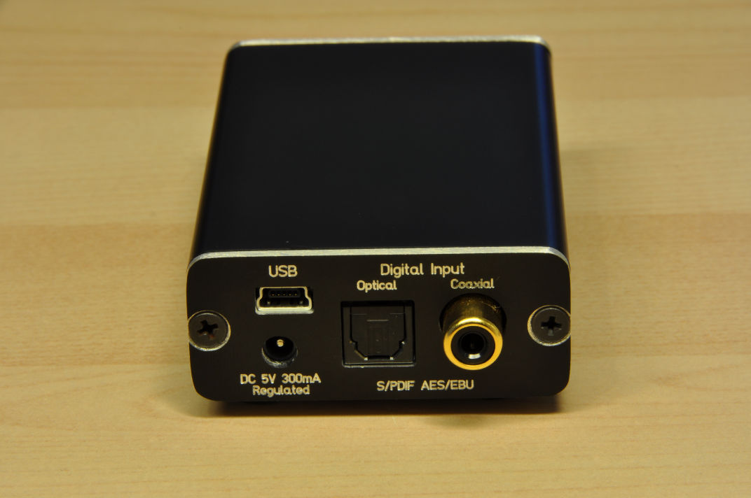
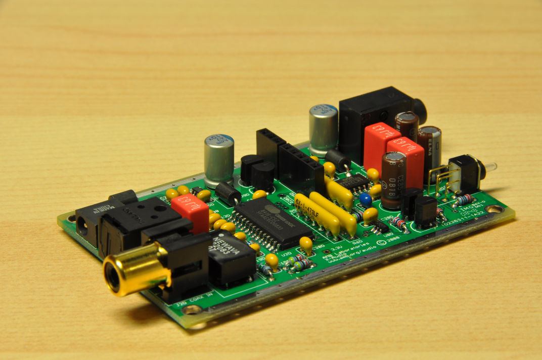
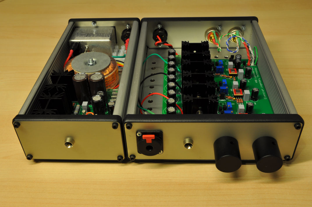
The populated PCB looks different from the schematic to me as well.  Must have been fun soldering everything in such close proximity to each other. 
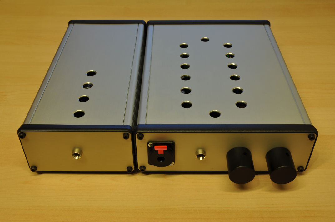
 
Jan 24, 2013 at 5:38 PM Post #8,897 of 9,811
You guys are missing the daughter board that's sitting up vertical in the middle of the larger PCB.
wink.gif

 
It's definitely nice work - love to see a packed case!
 
Jan 24, 2013 at 8:24 PM Post #8,898 of 9,811
You guys are right. The board in the first picture is his first version, shown beside the outline of his second version.
 
Yes his second version is actually larger than the first one. We're still trying to talk him out of it.
 
tongue.gif

 
The best part is, has tomb pointed out, that he's got 2 daughter boards sitting vertically in the middle of the main circuit. All that to cram more SMT components into a small volume. Because if there's still empty space somewhere, it's wasted space. Which is why I personally find it silly that after all that work, he went for a larger design.
 
Jan 24, 2013 at 8:51 PM Post #8,899 of 9,811
Quote:
You guys are right. The board in the first picture is his first version, shown beside the outline of his second version.
 
Yes his second version is actually larger than the first one. We're still trying to talk him out of it.
 
tongue.gif

 
The best part is, has tomb pointed out, that he's got 2 daughter boards sitting vertically in the middle of the main circuit. All that to cram more SMT components into a small volume. Because if there's still empty space somewhere, it's wasted space. Which is why I personally find it silly that after all that work, he went for a larger design.

Yeah - you're right - I missed the 2nd daughter board until I saw the pics in the other thread.
wink.gif

 
Jan 29, 2013 at 4:37 AM Post #8,904 of 9,811
You guys are right. The board in the first picture is his first version, shown beside the outline of his second version.

Yes his second version is actually larger than the first one. We're still trying to talk him out of it.


Not quite accurate, the second board design ( the outline in the pic) will not be any larger when finished than the current board. It simply allows for a larger battery at the expense of slightly less room on the PCB for op amp power rail caps. There are two daughter boards, one has the op amps and most of the feedback resistors, the other has most of the discrete buffer components. It is a very compact design.
 
Jan 29, 2013 at 4:51 AM Post #8,906 of 9,811
There is a larger case I could use;


But the only real advantage it has would be to allow for a 4 cell battery pack. I doubt I will use it. Hopefully I will be putting another amp together this week. I will try to get better pics of the assembly process.

Next PCB order will be an updated design very similar to the boards in the pictures, as well as one similar to the print out in the first pic. The new boards will have removable op amp daughter boards as well :wink:

Next step will be designing the front panel with FPE.

Joe
 
Jan 29, 2013 at 5:40 AM Post #8,909 of 9,811


Little better pic of the case and plastic chop job of a FP, AA sized battery to show some scale.

Where do you purchase most of the electrical components? How much have you spent on that project so far?
 

Users who are viewing this thread

Back
Top