


- Joined
- Jun 3, 2014
- Posts
- 707
- Likes
- 1,442
Introduction, Factory Front and PCB Area
Recently, I had the chance to go on a trip to China. I also happened to be visiting in the Guangzhou, Guangdong area (very southern part of China, little bit north of Hong Kong) where FiiO was located. Realizing there was an opportunity, I contacted the company and managed to set up a factory visit. Thanks to Sunny, James, and the rest of the staff at FiiO for being accommodating and making my visit a pleasant one!
Some notes before I begin – I only had a point-and-shoot camera on me for convenience. Combined with my non-professional shooting skills, I apologize for any bad quality photos.
I also apologize if I seem to ramble or for any poor organization in these posts – it’s my first time doing such a thing!
Also, these are only some of the photos that I took while there. If anybody has requests for anything else they would like to see, I’ll see if I took a picture of it and post it up later. If anybody has any questions in general, feel free to ask.
This is the first post in a series of posts. To jump to any other posts, click on the links below.
Post 1: Intro, Factory Front and PCB Area
Post 2: Final Assembly Area
Post 3: Repairs, Final QA, and Stress Testing
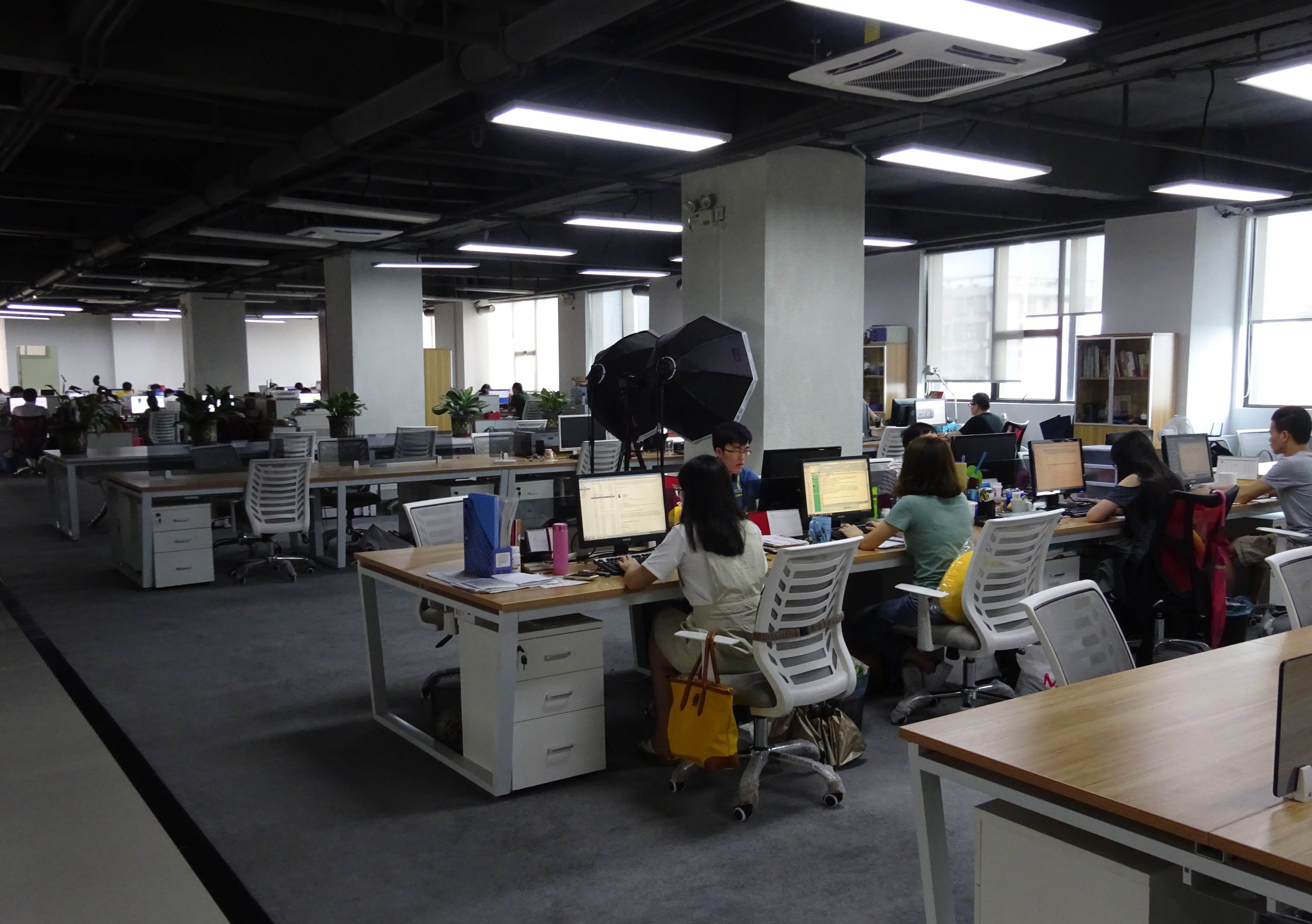
Post 4: Offices
Post 5: Chat with James Chung, CEO of FiiO
Factory Front


 Attaching screens to X1 PCB’s to facilitate loading of firmware. Screens will later be taken off before final assembly, where they will be put back on.
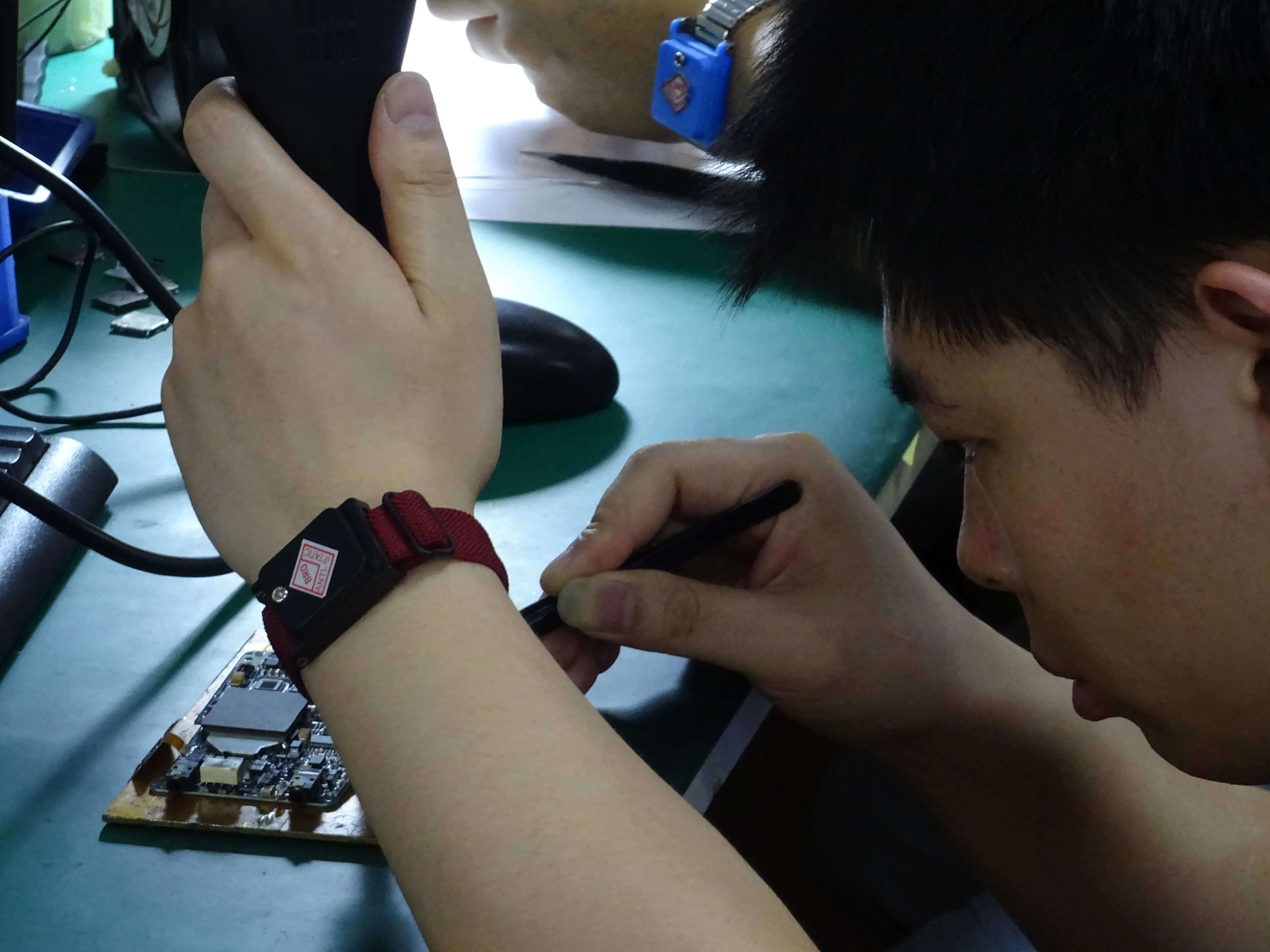
 X1 PCB’s being inserted with firmware. At this point screens are temporarily attached to PCBs to facilitate this process and to catch any potential problems with those parts now.
Recently, I had the chance to go on a trip to China. I also happened to be visiting in the Guangzhou, Guangdong area (very southern part of China, little bit north of Hong Kong) where FiiO was located. Realizing there was an opportunity, I contacted the company and managed to set up a factory visit. Thanks to Sunny, James, and the rest of the staff at FiiO for being accommodating and making my visit a pleasant one!
Some notes before I begin – I only had a point-and-shoot camera on me for convenience. Combined with my non-professional shooting skills, I apologize for any bad quality photos.
I also apologize if I seem to ramble or for any poor organization in these posts – it’s my first time doing such a thing!
Also, these are only some of the photos that I took while there. If anybody has requests for anything else they would like to see, I’ll see if I took a picture of it and post it up later. If anybody has any questions in general, feel free to ask.
This is the first post in a series of posts. To jump to any other posts, click on the links below.
Post 1: Intro, Factory Front and PCB Area
Post 2: Final Assembly Area
Post 3: Repairs, Final QA, and Stress Testing
Post 4: Offices
Post 5: Chat with James Chung, CEO of FiiO
Factory Front
FiiO’s factory is located in a nondescript building in a somewhat out-of-the-way area. This is how we know we’re here!
Right next to it is a statement of FiiO’s company culture and values
Assembly Floor 1 - PCB Area

