Alex let me know that he had started this thread.
The link posted above also has the Gerber files for the PC board, which anyone can use to have their own PC boards made at their favorite PC board fabrication house. The board is 4 layers.
I designed this amp mainly out of curiousity. I've wondered pretty much ever since the original O2 headphone amplifier was introduced what an inverting version would sound like. I discussed it with the designer via PM on another forum a few days after he released the O2, had he considered inverting. He said that he actually had. The non-inverting design was simpler and potentially lower noise due to the larger resistors required with the inverting configuration (Johnson noise) but he said maybe in the future he would consider an inverting amp. Well, this one is a version of such a thing. Same essential structure of his O2, with an initial gain stage followed by the cap-coupled pot in the middle and an output buffer stage. But to stir things up a bit I've used FET-input op amps for both stages, vs. the bipolar input in the O2.
This site has a pretty good explaination of the inverting op-amp configuration:
http://www.electronics-tutorials.ws/opamp/opamp_2.html
The inverting and non-inverting op-amp inputs are held at ground, which eliminates any common-mode distortion. With the more common non-inverting op-amp configuration (what is used in the O2 headamp and most other headamps) there will be a small common mode voltage.
An inverting op-amp configuration is also stable with a voltage gain less than 1, whereas a non-inverting op-amp configuration isn't stable at less than unity gain. The low-gain setting with the BOM values for this amp has a voltage gain of 0.75x (attentuation), then the output stage has a gain of 1.3x. Multiply those and you get 0.75 * 1.33 = 1x, same final result as the O2 low gain (the most common way people build it up). then in the high gain you get 1.87x, times the 1.33x output, = 1.87 * 1.33 = 2.5x, again same as the O2 in the high gain position.
And of course with the two inverting stages in series in this amp, the net result is a non-inverted signal, same as the O2 headamp.
I "fixed" some other annoyances I've had with the O2 over the years:
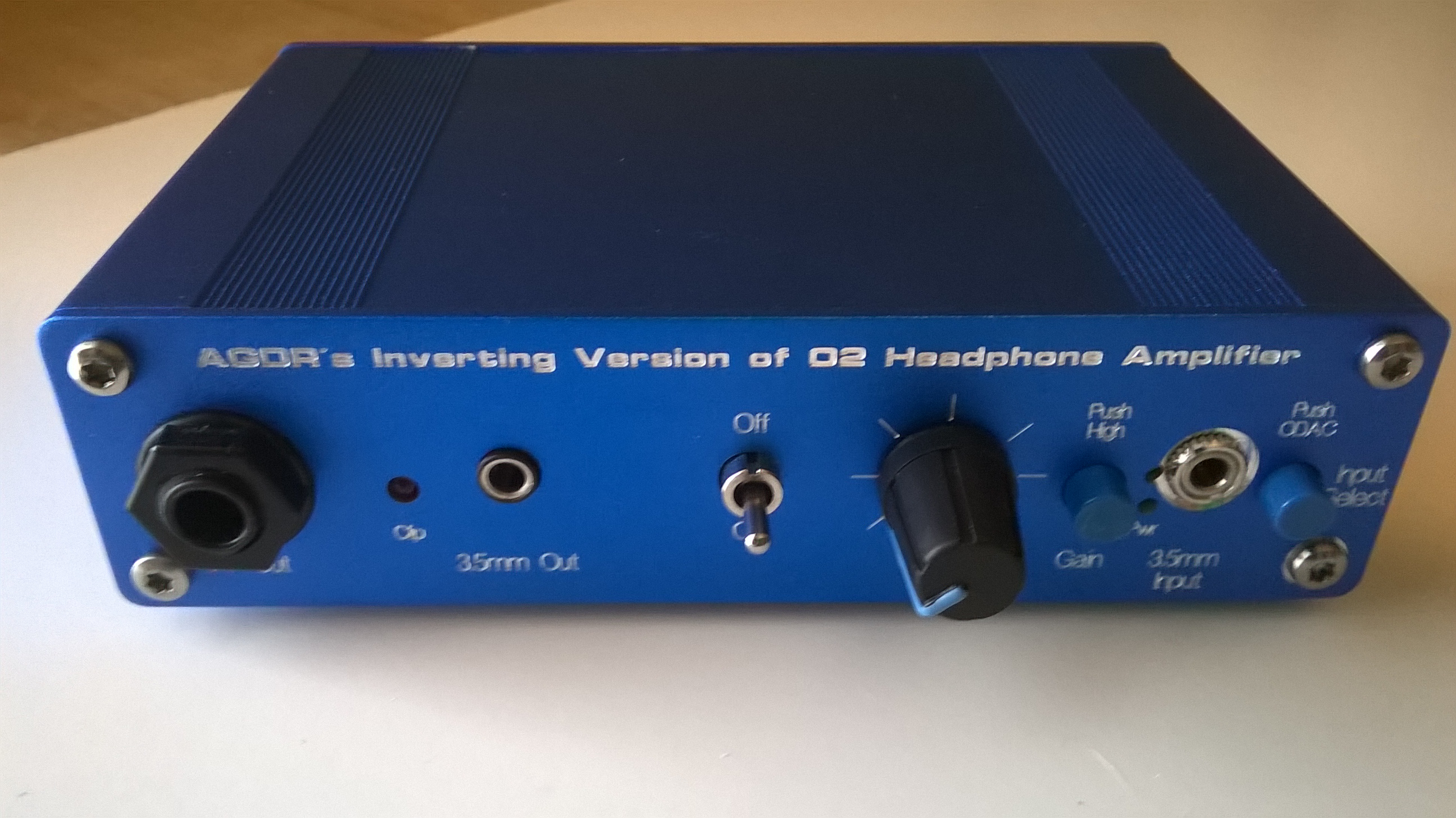
* power jack in the back
* voltage regulators heat sinked to the rear panel, which means that both front and rear panels have to be drilled (which is why the designer put his jack in front, to reduce panel costs).
* toggle power switch rather than slide to help the two power rails disconnect at the same time
* Includes a headphone relay for zero turn-on and turn-off thumps. The power management circuit was trying to do several things at once, including thump elimination, and IMHO it didn't do any of them especially well.
* power LED on each rail to help diagnose when a power rail is lost. This comes from helping a ton of people fix their O2's over on another forum over the last few years. One of the first things I often have people do is check their power rails.
* Input select switch and separate PCB holes for switching between the front panel 3.5mm jack and the ODAC board.
* 1/4" output jack, along with the 3.5mm jack
* heat sinked 250mA buffer chips. There is a known problem with the O2 where 16 ohm headphones that are low sensitivity, combined with high volume and music with high peaks can overheat the NJM4556A chips in the O2 and cause them to crack in half. The O2 has 140mA maximum, this one has 250mA.
* +/-15.3Vdc power rails vs. the +/-11.6Vdc in the O2 (12V minus the Shottky diodes minus the PM mosfet voltage drop). That is 3 extra volts of voltage swing for high impedance headphones that need more voltage swing. Higher chip voltage also helps reduce chip THD by a tiny amount.
* Low-dropout low(er) noise adjustable voltage regulators vs. the fixed 12V vregs in the O2 headamp. Note - these are only lower noise if the set resistors are noise bypassed with a capacitor, per the data sheets, which I've done. The very low noise figure given for both chips (LT3015 and LT3080) in the data sheets is actually for the minimum adjustable voltage, about 1.8V or so, and that noise "gains up" with increasing voltage unless bypassed. This is something that isn't terribly clear from the datasheets (the given noise is for the lowest possible output voltage) but I've confirmed it with the LT applications engineering folks.
* has power rail clamp diodes so a lost power supply on one rail won't cause a high reverse voltage on the other, something that has wiped out U6 for folks in the O2 headamp on occasion.
* includes a clipping indicator circuit and LED so you know when the input stage (or output stage, I sense both) are being overdriven. That is another one of the things is asked/suggested to the designer a couple of days after he released the O2. His reply was simply no space left on the PC board to add any more parts.
* 5K pot vs the 10K in the O2, combined with a lower 24.9K ground return resistor (5x the pot to prevent loading) vs. 40.2K in the O2, to lower Johnson noise. A 5K works here because the LME49880 gain chip is THD+N specified down to a 600 ohm load. The NJM2068 in the O2 is only good for a 2K load. The coupling cap here is bumped up to 4.7uf vs. 2.2uF in the O2 to keep the frequency response the same with the lower value of ground return resistors.
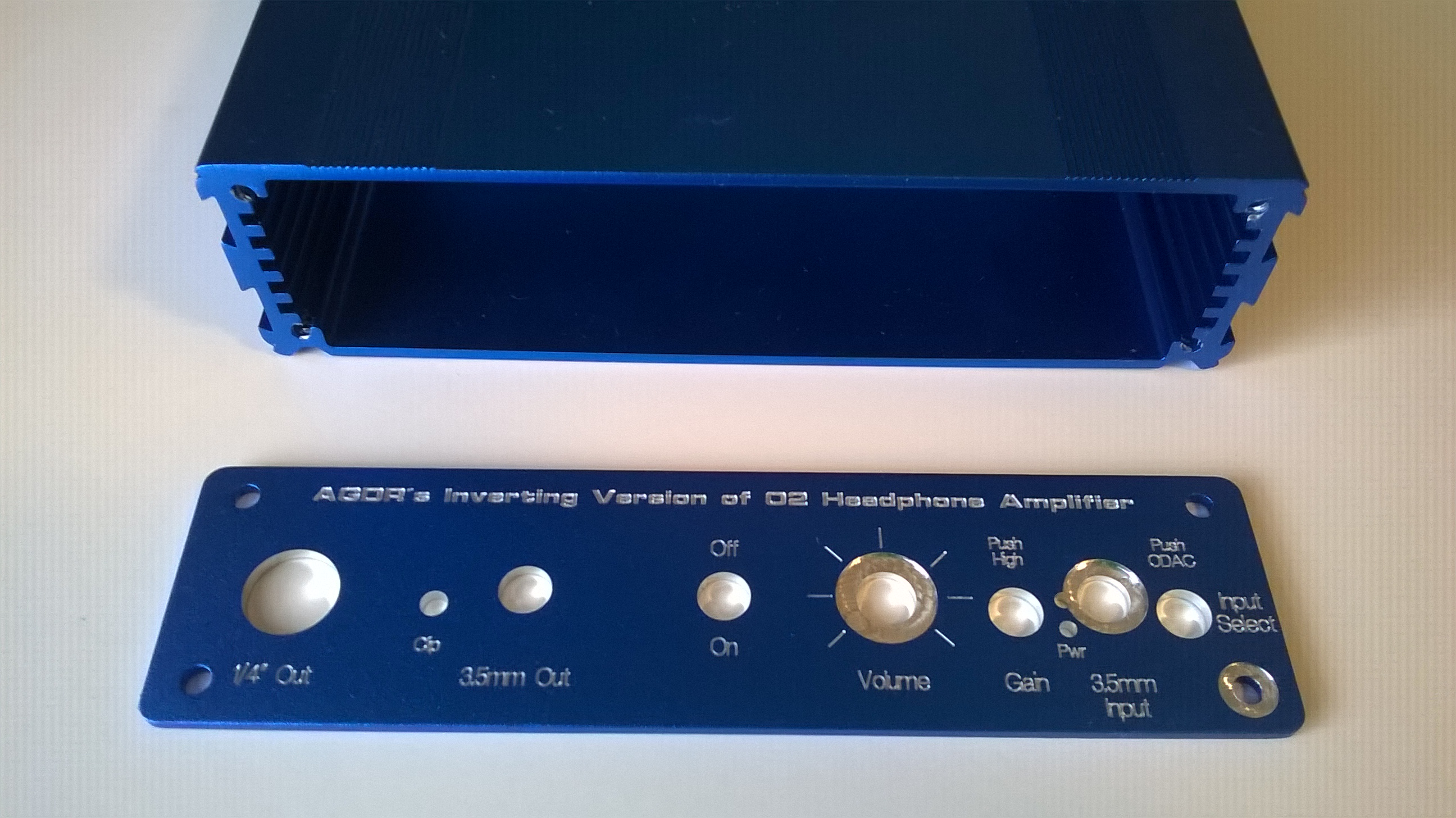
* But... no batteries! This one isn't "transportable". And this one uses the B5-080 case which is about 1 inch wider than the B2-080 used with the O2 headamp. That allowed more front panel room for thngs. No batteries means no power management circuit, as in the O2, I actually had one designed an on the board at one point, back when I was considering having batteries, but it wound up as all surface mount to fit. Without the PM circuit 95% of this board is now through-hole parts, making it easier to solder, like the O2.
I know that Alex is building one of these. If anyone here has a board made and builds one, please post some pictures and listening impressions!