


cyanoacry
New Head-Fier
- Joined
- Mar 16, 2005
- Posts
- 14
- Likes
- 11
Hi all,
I designed a electrostatic headphone amplifier with a couple goals in mind:
The end result was a high-gain voltage amp (around 60dB of gain), but it was extremely non-linear due to the huge capacitances of the main NPN BJT involved: Fairchild's KSC5027. And that's despite operating in class A!
The solution was to apply large amounts of feedback (20dB) and do some analysis to ensure stability and phase weren't a problem. End result is a 40dB amplifier that has relatively OK specifications, and sounds great (as far as I've tested, anyway, numbers forthcoming).
Quick stats (simulated):
Amplitude: +/-400V (1500Vpp stator-to-stator)
Distortion: <0.1% 0-20KHz at 300Vpp on a single output
Frequency response: 0-50KHz +/- 1dB
Open-loop gain: 69dB
Closed-loop gain: 40dB, 60 degree phase margin
The amplitude and distortion measurements check out as far as my scope goes, but I haven't had the time to hook it up to a proper analyzer yet.
Since this was the result of a school project, I've got some documentation available (and the whole shebang) at https://bitbucket.org/cyanoacry/ee91
Unfortunately, 2/4 stator boards have blown due to insulation problems (that's me being cheap and forgetful with space), so I'll be designing a proper second round of boards.
For convenience's sake, all KSC5027 output transistors and the power-supply FETs were watercooled using a Koolance setup. There's no need for it, but I wanted to play around with watercooling some day...
Pics:

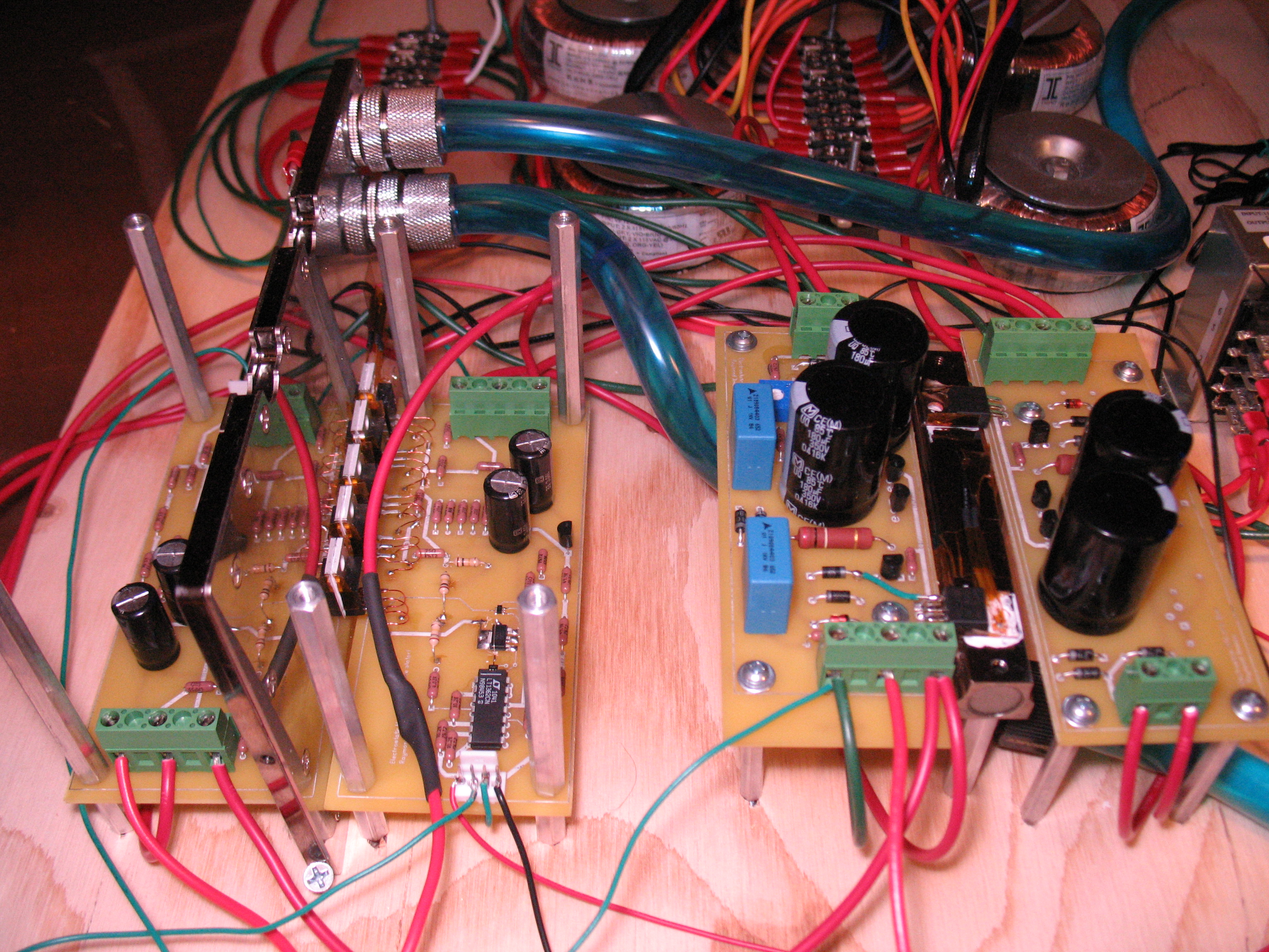
Overall view of the setup (messy, I haven't cased it, I know)

Close-up view of a single stator board and the watercooling setup

Another view of the stator boards (2/4) and the power supply. The dual toroids per rail can be seen in the background.
Schematics/docs:
I'm interested in making this amp better, so please give me your feedback. It's my first design, so sorry if there are any rookie mistakes! [size=small]m(_ _)m[/size]
[size=small]Edit: fixed amplifier/power supply schematic to match documentation.pdf (correct version)[/size]
I designed a electrostatic headphone amplifier with a couple goals in mind:
- cheap parts, no specialty items, all available from Digi-Key (in stock!), including transformers
- good sound no matter the component tolerances
The end result was a high-gain voltage amp (around 60dB of gain), but it was extremely non-linear due to the huge capacitances of the main NPN BJT involved: Fairchild's KSC5027. And that's despite operating in class A!
The solution was to apply large amounts of feedback (20dB) and do some analysis to ensure stability and phase weren't a problem. End result is a 40dB amplifier that has relatively OK specifications, and sounds great (as far as I've tested, anyway, numbers forthcoming).
Quick stats (simulated):
Amplitude: +/-400V (1500Vpp stator-to-stator)
Distortion: <0.1% 0-20KHz at 300Vpp on a single output
Frequency response: 0-50KHz +/- 1dB
Open-loop gain: 69dB
Closed-loop gain: 40dB, 60 degree phase margin
The amplitude and distortion measurements check out as far as my scope goes, but I haven't had the time to hook it up to a proper analyzer yet.
Since this was the result of a school project, I've got some documentation available (and the whole shebang) at https://bitbucket.org/cyanoacry/ee91
Unfortunately, 2/4 stator boards have blown due to insulation problems (that's me being cheap and forgetful with space), so I'll be designing a proper second round of boards.
For convenience's sake, all KSC5027 output transistors and the power-supply FETs were watercooled using a Koolance setup. There's no need for it, but I wanted to play around with watercooling some day...
Pics:
Overall view of the setup (messy, I haven't cased it, I know)
Close-up view of a single stator board and the watercooling setup
Another view of the stator boards (2/4) and the power supply. The dual toroids per rail can be seen in the background.
Schematics/docs:
I'm interested in making this amp better, so please give me your feedback. It's my first design, so sorry if there are any rookie mistakes! [size=small]m(_ _)m[/size]
[size=small]Edit: fixed amplifier/power supply schematic to match documentation.pdf (correct version)[/size]

") My goal here was to make something a little like an upgraded eXStatA, now that the KSC5042 is out of production.
My goal here was to make something a little like an upgraded eXStatA, now that the KSC5042 is out of production. 