My first amplifier design
Jun 8, 2004 at 11:43 PM Thread Starter Post #1 of 24

taylor

1000+ Head-Fier
Joined
Feb 6, 2004
Posts
1,089
Likes
10
schematic1.jpg


I attempted to design a headphone amplifier.

It uses an op-amp with class-a bias, with a MOSFET buffer.

Capacitors: each channel uses 4 caps.
C1 is the input cap
C2 is the coupling cap
C3 is the output cap
C4 is the power supply cap
(Revision - I accidently included two pairs of C4 on the schematic, only one pair is needed)

Resistors:
R1 is the drain resistor for the opamp
R2 with R3 sets the gain
R3 with R2 sets the gain
R4 helps bias the opamp into class A
R5 is the drain resistor for the MOSFET
R6 is the gate resistor
R7 is the source resistor for the MOSFET
(Revision: I also forgot to add the volume control pot, it's wired in the usual way, where one lead is at the input, the other lead is at the ground, and the wiper is connected to the input of the opamp)

Semiconductors:
OPA1 is an opamp that provides gain
Q1 is the MSOFET buffer
Q2 and Q3 are the JFETs to bias OPA1 as per tangents guide.

Do you think this would work? What kind of values would I want for the components? Sorry if I asked a silly question, this is my first try at designing an amp.
 
Jun 9, 2004 at 1:46 AM Post #2 of 24
This may just be me, but doesn't having C1, C2, and C3 seem redundant? Unless you are using a really crappy op-amp, C1 should do the job fine by itself, unless I misunderstand something. I'd always been under the impression that putting capacitance after an op-amp causes ringing.

Also, (I've never tried this, but i intend to with my PPA-in-progress) you could feed back the output of the mosfet instead of the output of the op-amp, possibly improving linearity. This could potentially cause instability due to the phase lag of the mosfet, but it would be interesting to try
orphsmile.gif
This would also allow you to have a feedback loop before the MOSFET and after so you could have some Jung Multiloop action going on, much like in the PPA.

Also, are C1 and C4 connected in that picture? I would think you would want the signal input separate from the power rails.

What purpose does R7 serve? You should be able to just feed the mosfet directly from the positive rail without a resistor.

This is kinda nit-picky, but you have a P-channel mosfet in your diagram, and I believe you would want an N-channel for this circuit.

You might want to consider driving the mosfet with a low input capacitance JFET, just to prevent ringing due to the op-amp trying to drive the relatively high input capacitance of the MOSFET. See THIS schematic for the jist of what I am talking about.

Other than these nit-picky things, it seems like a pretty solid design! Obviously, you are gonna want to couple that with an equally solid power supply design though. The type of buffer design you are using has some pretty serious power requirements. From what I have heard the typical average draw is 100 mA per channel, and that can vary from 10 mA up to 200mA when you are driving a signal! You are gonna want some seriously hefty power caps for this baby if you want it you really churn out some good sound, and believe me it will
600smile.gif


You also might want to consider replacing R5 with an LM317 rigged as a current source. This will steady the power draw of the MOSFET out so you won't have the wild 10mA to 200mA fluctuations I mentioned above. However, supposedly LM317s add some high frequency noise to the signal. I have yet to test this, though I will be doing so in the next few days when my last shipment of parts for my buffers arrive
biggrin.gif
 
Jun 9, 2004 at 4:52 AM Post #4 of 24
It is a single ended design guys... caps will have to be in the signal path....

Regardless of the opamp, C3 MUST and I repeat *MUST* be there unless your cans like 5-10 volts across them. Again, this is a single ended design... there is no chance for voltage cancellation that would negate the voltage and make it can-friendly. C2 should probably also be there to make sure the gate is DC-free... which may matter depending on how the MOSFET is biased. C1 at the opamp could be omitted, I suppose, since amplified DC from the opamp will be blocked by C2 before it reaches the MOSFET.

Include feedback? You could do this... Sheldon Stokes does this in his SDS amp... but notice his push-pull output stage. That is why he manages no output cap. The inverted voltage from one MOSFET effectively cancels the voltage of the other across the headphones.

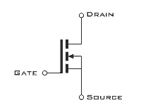
BTW- nothing wrong with P-channel, though most like N-channel MOSFETs better. The way it is wired now, you are taking the output signal from the MOSFET's drain, which will give you voltage and current gain. I am guessing this is what you were going for in selecting the P-channel FET. Nelson Pass does this in his amps, and I usually try to in my work with MOSFETs.

Don't worry about the JFET up front... the opamp has a low enough output impedence that there should not have any adverse effects from driving it direct without a JFET buffer. The JFET was added because the original Szekeres design, which used a single N-channel MOSFET providing current-gain only, was intended to be driven directly by a 10k volume pot from the source... no preamp/opamp involved in between. By using this opamp, you eliminate the high-frequency roll-off problems associated with driving the high gate-capacitance FET with a high-impedence source.

I sort of agree with using a constant current source... but disagree with LM317 after having read about it. It is basically another IC... and being the Zen-minded parts minimalist I am, I do NOT like IC's in the signal path anymore. Why use an IC with 5+ gain stages when one will do? You could use another MOSFET as the current source, but a high power resistor would do just fine, really.

On another note, you may check out Marcello Pellerano's Zen amp, which is a scaled down model of Nelson Pass's Zen amp. It utilizes a constant current source that varies based upon the load... and also uses a N-channel device wired for voltage and current gain, as your is. If you require more voltage gain, you can add a simple N-channel FET buffer up front wired for voltage gain and you will get plenty of power to drive any cans.

Another thing to consider... you might look into some of Neslon Pass's documents about his amps. You could use the Son of Zen or X-Son of Zen design to eliminate output caps. His Zen variation 5 (push-pull complimentary) would also do this. Then you don't have to worry about those nasty electrolytics in the signal path (not actually so bad, though, really... and I hate caps in signal path).

If you want more MOSFET ideas, look at these:

Zen headphone amp
Szekeres
Murdey amp
Newer Zen variations
Older Zen variations

(note: amp designs found with last two links probably MUST be modified for headphone use)

And, check out the DIYAudio Forums Pass Labs section for more help.
 
Jun 9, 2004 at 10:55 AM Post #5 of 24
I suppose I did use the wrong symbol for the MOSFET. It should be a N-type one, since I do not want any voltage gain. The op-amp will give me all the voltage gain I need, the MOSFET is just a buffer to add more power to the output.

Would reversing the arrow work for making it into a N type?

I did not know that using a P-type MSOFET gave voltage gain, would it be a good idea to replace the op-amp with a P-type MOSFET for voltage gain then use the N-type MOSFET for current gain?

schematic2.jpg
 
Jun 9, 2004 at 5:27 PM Post #6 of 24
It is not the channel of the MOSFET itself that yields voltage gain... it is how it is wired. The way you have the MOSFET drawn in your second drawing is called common drain. This gives only current gain when the output is taken from the source of the FET. The mode that gives current and voltage gain is common source, with the output taken from the drain (how it was with the P-channel FET since the polarity of the FET is reversed).

If you wanted to get rid of the opamp and its many gain stages (not especially good for extreme hi-fi), you wire two FETs in common source mode, which would give you a voltage gain front driving a voltage and current gain buffer on the output. You could also use a tube up front... heh

For all intents and purposes, however, the opamp in there is just fine and will feel right at home running class A and driving the FET follower. Should sound pretty good, too.

For more info about MOSFETs and such, see Nelson Pass's article about MOSFETs. (VERY helpful) (hmm.... seems they updated and changed this article... if you want the original, I have it)
 
Jun 9, 2004 at 5:33 PM Post #7 of 24
I've become a minimalist. Some op-amps don't need a current source to bias them class A. Also, I've found that I don't need (voltage) gain in my amplifier. So, I recommend simply buffering the signal to your headphones. Try a MOSFET follower (or a JFET follower, or a BJT follower).

Unless you use the top 10% of the volume control setting (without gain), probably don't need added gain...


JF
 
Jun 9, 2004 at 5:37 PM Post #8 of 24
Agreed.

However, if you do find that you need voltage gain as well, you don't need to dispair because you can wire the MOSFET to give both current and voltage gain... and then you only have one device in the signal path. (well, as far as the amp is concerned... who knows what is in that CD-player, etc.)
 
Jun 9, 2004 at 8:04 PM Post #10 of 24
After making plenty of measurement to make sure you're not going to damage your setup, give it a listen.

mosfet_n_chan.gif


BTW: I'm not that familiar with MOSFETs, I went with JFETs...kind of like:
attachment.php


JF
 
Jun 9, 2004 at 8:20 PM Post #11 of 24
quote
C's in the signal path
eek.gif


There are at least 2 caps in the signal path of your rudistor
eek.gif
 
Jun 9, 2004 at 8:30 PM Post #12 of 24
Quote:

Originally Posted by kevin gilmore
quote
C's in the signal path
eek.gif


There are at least 2 caps in the signal path of your rudistor
eek.gif


Being the skeptic I am, can you kindly point out where you got a schematic for Rudi's amp? I understand that you built one, but with what schematic to guide you?

I'm not trying to start a war again, just looking for some facts.
 
Jun 9, 2004 at 9:05 PM Post #13 of 24
I built the electrostatic amp, the schematic of which is published on
the rudistor site. There is one capacitor in each electrostatic element
drive between the first and second stage. This is their electrostatic
amp. There are 2 capacitors in the signal path per channel.
http://www.rudistor.com/sound-lab/heurideng.htm

The amplifier gsferarri has is the dynamic amplifier. It has a tube
front end and a single bipolar transistor as the output stage. From
the pictures gsferarri has posted it is absolutely obvious that there
is a coupling cap (the big yellow thing) and there is an output cap
(the brown electrolytic). It does not take a brain surgeon to draw
out the schematic from the pictures supplied.
http://www.matcha-tea.com/files/othe...0Reference.pdf

Anyone notice the perf board with the input pot on it. Anyone notice
the quality of the input pot. Anyone notice the extra copper heatsink
added. Anyone notice the board is single sided with no ground plane.
How about the extra shield added around the input pot? Anyone
notice that the yellow cap is way to big to fit in the hole it was
designed for? Some say this unit has audible hum. Is it any surprise
when the input wires go right past one of the tubes??
This is a professionally built product???

You certainly don't see this level of quality in headroom products. Nor
in anything jan meier would build. Even the ppa's are of a much higher
build quality than this. Now early singlepower units had air wiring...

But it does have Induced Harmonic Compensation whatever that series
of non-coherent buzz words mean. .2% thd --- yikes. Whats the
thd of a ppa?? like <.005??

Bandwidth of 0 to 50hz maybe 0 to 50khz??

Go ahead and flame away...
 
Jun 10, 2004 at 12:04 AM Post #14 of 24
Noting the N-channel diagram posted above, you can see which is the source, drain and gate. MOSFETs in fact only have three connections. The center with the arrow is connected to the source. When using an N-channel device, the drain receives the positive voltage supply, while the source is grounded. Input is taken on the gate.

If you want to wire an N-channel FET for voltage and current gain, you need to ground the source directly, take input on gate, and output from the drain. A resistor connecting the drain to V+ provides the bias.

In your diagram, you basically have the MOSFET backwards... as the source is shown getting V+. I am guessing this is just because of the image being used... and not that that is how it is or will be.

If you go with the two FET design, the first FET does not need as high of a bias, and also needs to be a smaller FET (a ZTN3310 would probably work well) that has very little gate-source capacitance. The second FET would probably be best as an IRF510, IRF610, or equivalent.
 
Jun 10, 2004 at 1:55 AM Post #15 of 24
Quote:

Originally Posted by kevin gilmore
I built the electrostatic amp, the schematic of which is published on
the rudistor site. There is one capacitor in each electrostatic element
drive between the first and second stage. This is their electrostatic
amp. There are 2 capacitors in the signal path per channel.
http://www.rudistor.com/sound-lab/heurideng.htm

The amplifier gsferarri has is the dynamic amplifier. It has a tube
front end and a single bipolar transistor as the output stage. From
the pictures gsferarri has posted it is absolutely obvious that there
is a coupling cap (the big yellow thing) and there is an output cap
(the brown electrolytic). It does not take a brain surgeon to draw
out the schematic from the pictures supplied.
http://www.matcha-tea.com/files/othe...0Reference.pdf

Anyone notice the perf board with the input pot on it. Anyone notice
the quality of the input pot. Anyone notice the extra copper heatsink
added. Anyone notice the board is single sided with no ground plane.
How about the extra shield added around the input pot? Anyone
notice that the yellow cap is way to big to fit in the hole it was
designed for? Some say this unit has audible hum. Is it any surprise
when the input wires go right past one of the tubes??
This is a professionally built product???

You certainly don't see this level of quality in headroom products. Nor
in anything jan meier would build. Even the ppa's are of a much higher
build quality than this. Now early singlepower units had air wiring...

But it does have Induced Harmonic Compensation whatever that series
of non-coherent buzz words mean. .2% thd --- yikes. Whats the
thd of a ppa?? like <.005??

Bandwidth of 0 to 50hz maybe 0 to 50khz??

Go ahead and flame away...


Could you please enlighten me as to how your post has anything to do with my amp?

To reduce the bias, i'm assuming that means making R2 smaller?

Thanks for the advice on MOSFET choices.

When I get the chance (probably tomarrow, as the PC containing all my schematics is currently in use by my brother) i'll make the diagram correct, and include the type of MOSFET.
 

Users who are viewing this thread

Back
Top