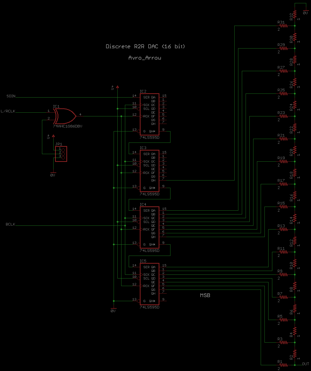
Circuit description:
Lets start with Left and Right channel selection.
The circuit shown is for just one channel.
The other channel is identical.
The L/Rclk signal lets us know which channel is being transmitted.
We are inputting an I2S signal and for that, when L/Rclk is low,
the Left channel is being transmitted and when L/Rclk is high,
the Right channel is being transmitted.
By using a 2 input Exclusive OR logic chip, we can select the
correct data. When both inputs match, either high or low, the
XOR makes its output low. If the don't match, the output is high.
In the circuit, we can select one input to be either high or low with
a jumper. When the L/Rclk signal matches the jumper, the XOR
output is low.
While the output is low, data can be clocked into the shift registers.
Now for the shift registers.
The shift registers clock in data when the output of the XOR
is low, and present it on their outputs when the XOR goes high.
For each "word" (left and right data), the bit clock (Bclk) cycles
64 times (64 Fs). In order for MSB to end up in the same place each time,
we have to have a total of 64 shift registers (32 for the left, and
32 for the right. Also, I2S waits one cycle of Bclk before transmitting
the first bit of information, so you can't use the first shift register.
That is why in the circuit diagram, Qh on IC5 is not used.
The 74*595 have eight registers each, so four are needed.
Is that enough to go on?
The data sheets can provided detailed descriptions of the inner
working of the logic chips used.